Well Intel recently announced their latest generation of CPUs and they are looking right at the cutting edge with multiple jumps including PCIe 5.0 and DDR5 being included with the new 12th generation of CPUs. So much so on the cutting edge that our coverage is a little late after trying to get in DDR5 memory to test with. So forgive the tardiness, but today we are here to finally take a look at Intel’s new CPUs, DDR5, Z690, and their new socket as well. The 12th generation of CPUs which were formally known as Adler Lake take an all new direction, following what we have been seeing on the mobile market with low and high speed cores and I’m excited to put them to the test.
Product Name: Intel Core i9-12900K and i5-12600K Adler Lake
Review Sample Provided by: Intel
Written by: Wes Compton
Amazon Affiliate Links: i9-12900K and i5-12600K
Intel 12th Generation Core Desktop Processors
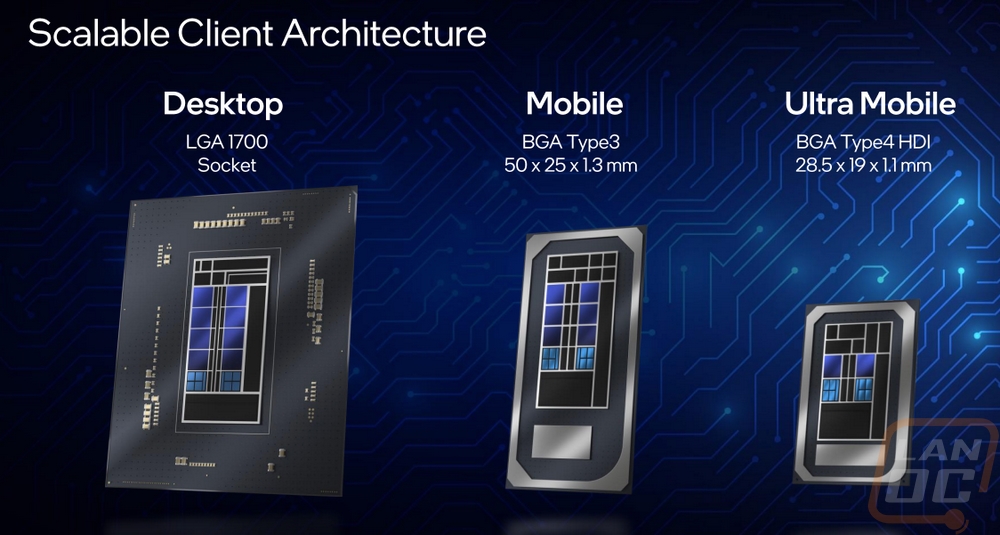
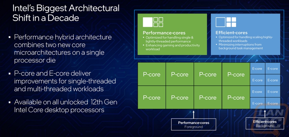
Before diving into the testing, I did want to take a closer look at what Intel has launched with the new 12th Gen Core CPUs. So let’s run through some of the information that Intel has released so we can get a better idea of what we are looking at. Like I said in the opening, the new CPUs aren’t just the same old design that we have seen for years now. Intel even refers to them as an SoC in their documentation here which is what mobile phone processors have been called for a while now. The CPUs are still multi-core, but in the past desktop CPUs would just get a specific number of cores, they would all run at nearly the same speeds with the exception of turbo clocks, use the same amount of power, and have the same design. The new design uses a combination of two different core designs now. Intel refers to them as P-core and E-Cores which makes it easy to keep track of. They have performance cores and efficient cores. The performance cores are similar to what we have seen in the past and are optimized for single-threaded or lightly threaded performance which to be fair is what PCs have been focused on for years. Fast gaming performance and productivity. The new e-cores open things up though. They are optimized for highly threaded workloads and are perfect for handling background tasks to help prevent slowdowns on the p-cores. They are also as the name would imply more power-efficient as well. This new architecture is designed not just for desktop and mobile use like in the past. They now have kept in mind ultra mobile, so in other words, they used to be good for PCs and laptops/compact designs like the NUC series. Now they are looking at mobile phones and similar devices.
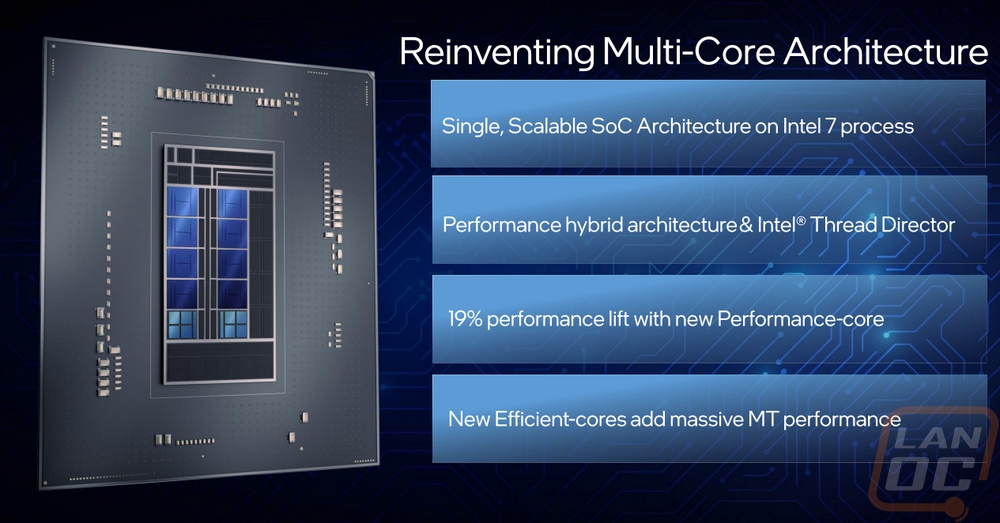
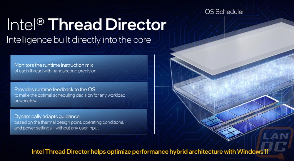
The big thing about running multiple core types like this though is that the overall performance depends highly on how applications and your operating system handle things. Without that control, your OS could give performance applications like games the e-cores and waste p-cores on small applications. Intel has worked with Microsoft to get their thread director tied in with the OS schedular in Windows 11 to do just that. It is constantly looking at current usage to help adjust and guide workloads to the different core types. This does mean that the 12th gen CPUs are best used on Windows 11 though so keep that in mind.
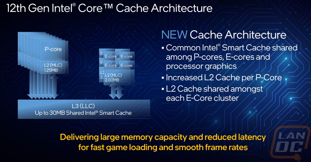
The Adler Lake CPUs also have a new cache architecture. The layer 2 cache for the P-cores is much larger and is dedicated per core. Then for the e-cores, they share a 2MB cache across four e-cores. The layer 3 cache though is shared and can be up to 30MB depending on the model.
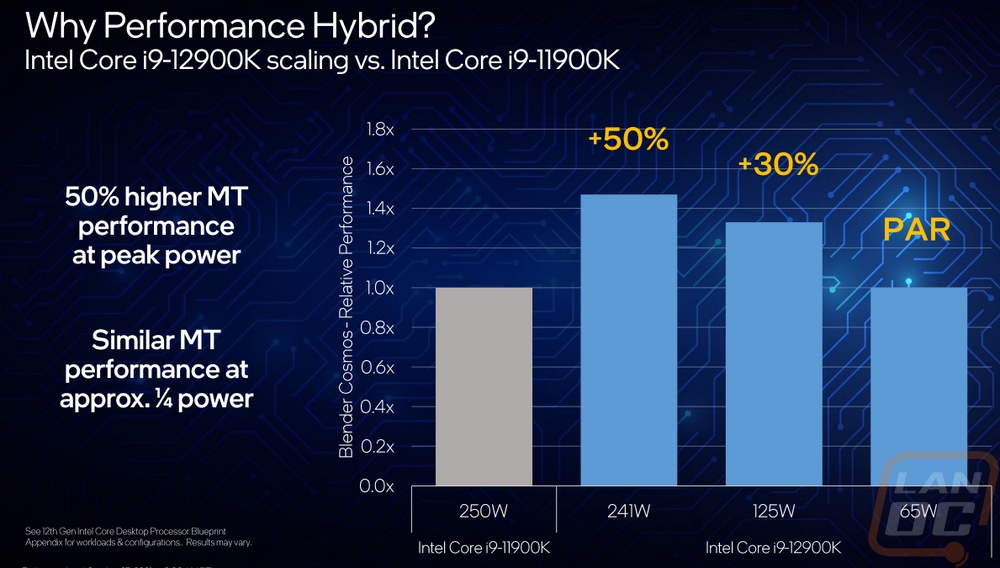
Intel did include a graph comparing the scaling between the new i9-12900K and the previous generation i9-11900K. This was specifically looking at blender performance and we will test that later. But the idea here was to show how the new 12900K can perform 50% better when using around the same wattage. But more importantly, using the mixed core types you can see a similar performance at a much lower wattage with it down to 65 watts at the same performance. I know for some enthusiasts, the fastest possible performance is all that is important and that is what has driven the PC CPU market up until now. But the mobile market on laptops and phones has had to also balance battery life which is why this hybrid design has been in mobile phones for so long now. But for me, I’m interested in my system not pulling big wattage numbers when I’m doing less demanding applications. Saving the power usage for when I’m in game or rendering for example. The energy usage would be nice, but I’m hoping it also means my PC will be quieter as well.
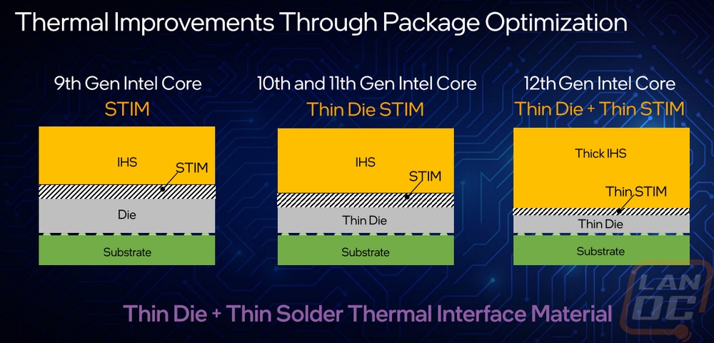
Speaking of thermals, they did make changes to the overall package as well. They now have a thick integrated heatsink with a thin die and thin thermal interface material, specifically a solder.
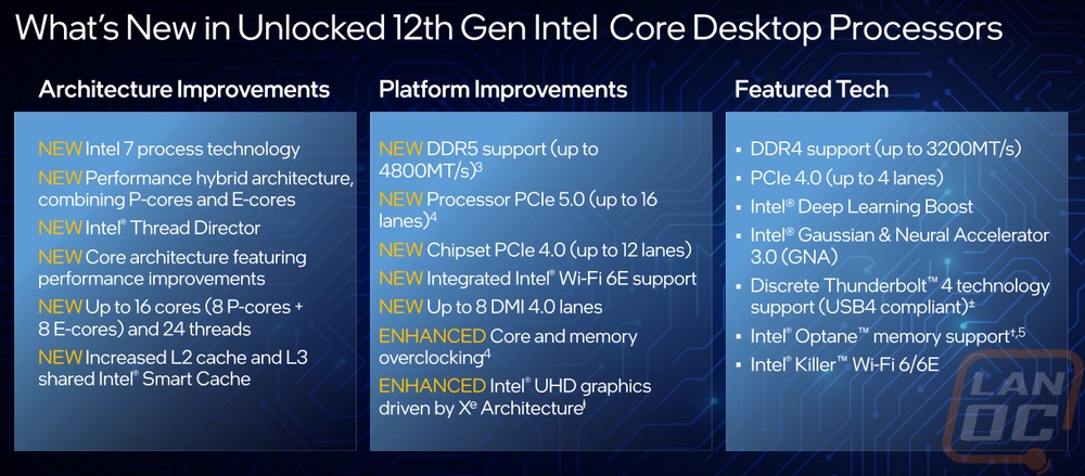
Intel also put everything together in one page to show off the improvements with the 12th gen CPUs and some of these are chipset specific which I will get into in a minute. But one I haven’t brought up yet is the Intel 7 process. Intel has been very slow to move to 7nm compared to the rest of the market but they have once again changed things up and they renamed their new Enhanced SuperFin process to 7 to show that they think their build process compares with a standard 7nm process when it is built at 10nm (which is a jump from the previous 14nm+++ process). In fact, on their roadmap, they have been showing off what they are calling Intel 4 which would be built at 7nm but has the performance similar to 4nm.
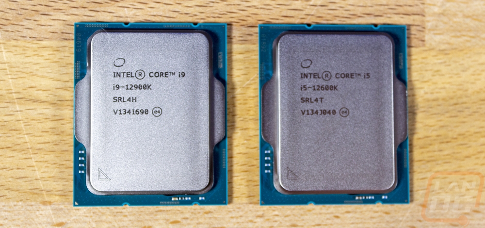
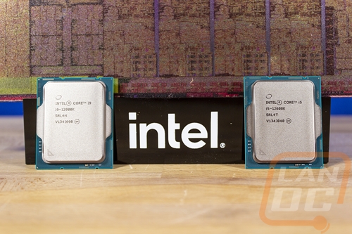
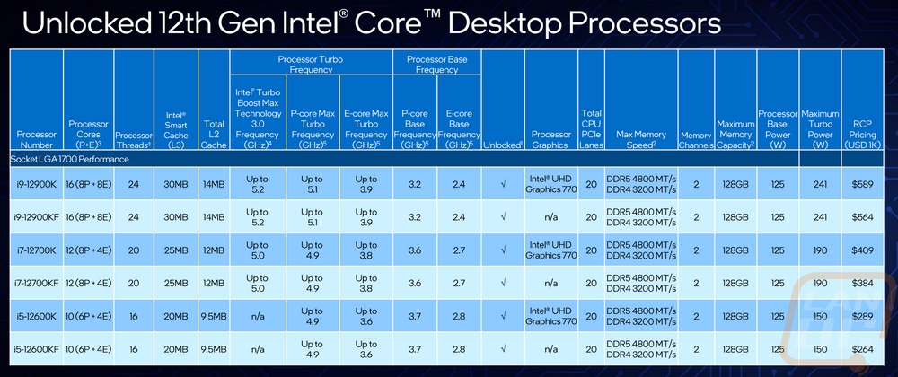
Before getting into a few other things I did want to finally look at the product stack for desktop processors. The previously mentioned i9-12900K is of course at the top, just like the 11900k/10900K/9900K all before it. The flagship processer has 8 of the performance cores and 8 of the e-cores. This and the similar 12900KF which is the same processor but without the integrated GPU both have a 30MB L3 cache and 14MB of L2 in total. With turbo boost max it will run up to 5.2 GHz and 5.1 GHz with the normal p-core turbo. Then the e-core will run up to 3.9 GHz. Their base clock speeds are 3.2 GHz for the p-core and 2.4 GHz for the e-core. All three of the K series processors with GPUs have the same UHD Graphics 770 which are nearly the same as the 750 from the 11th generation but with a higher boost clock speed of 1450 MHz on the 12600K and 1550 MHz on the 12900K vs 1300 MHz. All of the performance desktop processors support both DDR5 or DDR4 depending on the motherboard with a DDR5 speed of up to 4800 MHz and 3200 MHz for DDR4 before it is considered overclocking. Skipping the other KF processers, there is also the i7-12700K which has 8 P-cores and 4e-cores at a slightly slower 5.0/4.9/3.8 GHz boost for the Turbo Max, P-Core Turbo, and E-Core boost speeds. But the base speeds for the 12700K are higher than the 12900K at 3.6 for the P-Core and 2.7 for the E-Core. Then there is the i5-2600K which has 6 P-Cores and 4 E-Cores. This one doesn’t have a turbo Max clock but runs at 4.9 for the P-Core Turbo and 3.6 for the E-Core Turbo then is even higher on the base clocks at 3.7 and 2.8 GHz. All of the options have a base power of 125 watts but the flagship 12900K can have a max turbo power of 241 watts, 190 watts on the 12700K, and 150 watts on the 12600K.
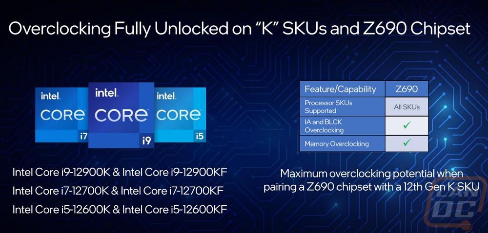
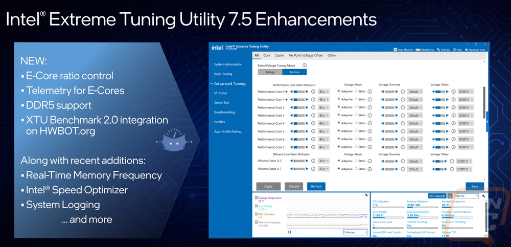
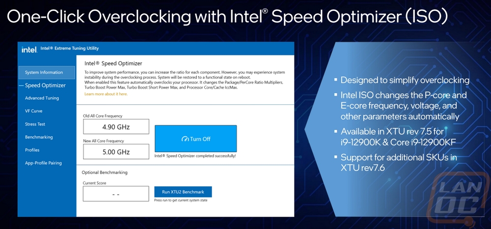
For overclocking the 6 CPUs listed above are all of their unlocked options as long as they are combined with the Z690 chipset. This means they have IA and BLCK overclocking as well as memory overclocking. Intel has also updated their extreme tuning utility as well to help support the 12th generation features. Specifically, they have added support for overclocking the E-Cores and DDR5 support. They also have integrated the XTU 2.0 benchmark on hwbot.org. For those of you who don’t want to get into the dials, they also have the ISO or Intel Speed Optimizer which will do a simple overclock for you. A lot of motherboards also have a similar option as well.
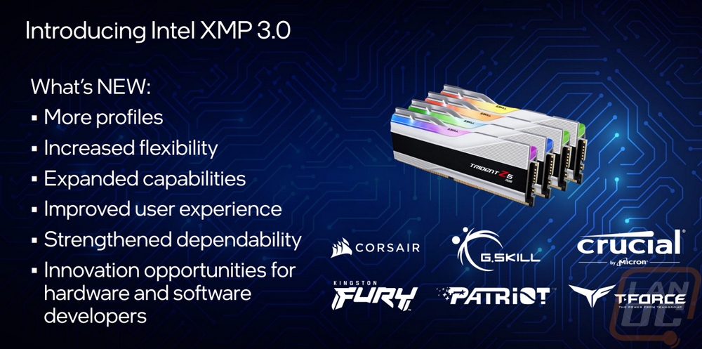
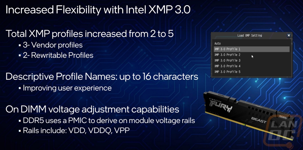
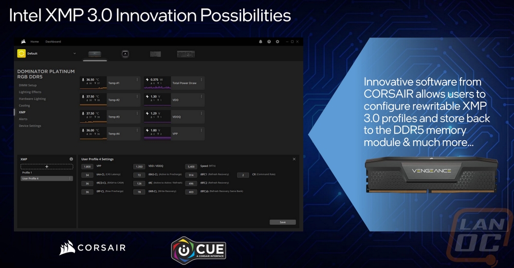
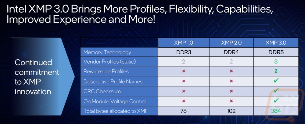
One of the big features introduced is of course the support for DDR5 memory. Both DDR5 and DDR4 are supported officially depending on the motherboard. Alongside of DDR5 Intel is also introducing XMP 3.0. 3.0 is DDR5 specific like XMP 2.0 was DDR4 specific and the original XMP was for DDR3 and has a few key features that help bring a lot more flexibility. In the past, you would have up to two profiles that have the memory kits clock speed and timings they are now expanding that out to 5. The old design had both profiles being vendor-specific and most used it to have your main overclocked profile and a slower option if needed. They now have the option to have three XMP profiles and then there are two new rewritable profiles. This means you can setup your own clock speeds, timings, and voltages and you don’t have to use a BIOS preset save to go back to it. In fact, it will move from computer to computer. You can also now name the profiles which help you figure out which is which as well. Memory companies can use their own software to control the profiles
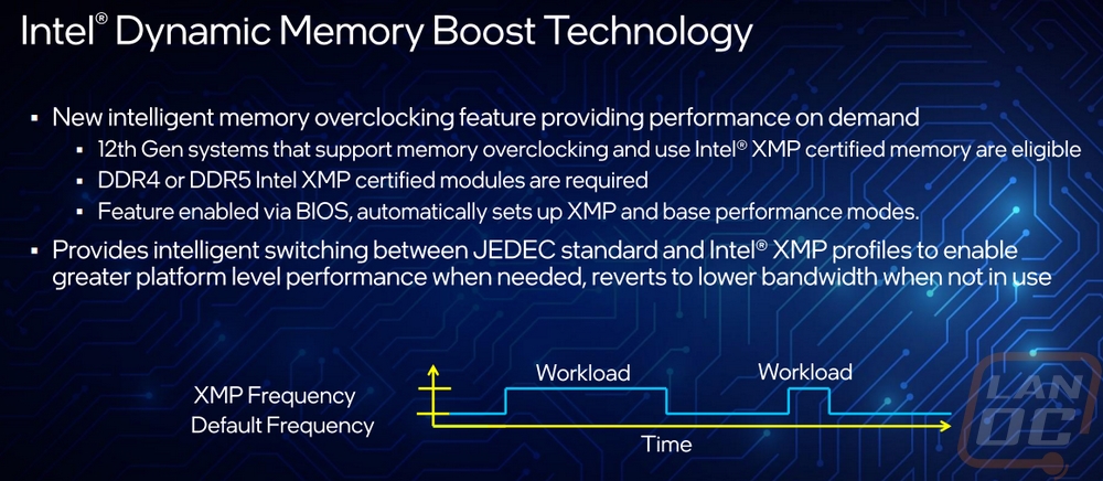
Also on the memory front, they now have Intel Dynamic Memory Boost which is a lot like how CPU clock speeds are handled. In the past memory, speed was set and that is it. But with CPUs, you have a base speed and turbo speeds that can spin up to higher clock speeds when your workload needs it. Dynamic Memory Boost can switch between the base JEDEC standard and one of your XMP profiles so you get the performance when needed but aren’t running overclocked all of the time.
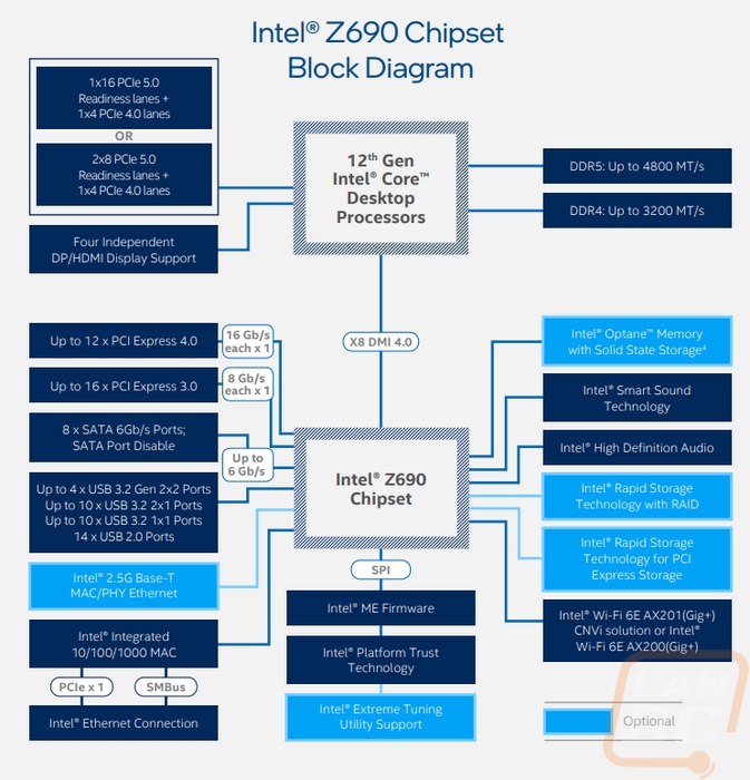
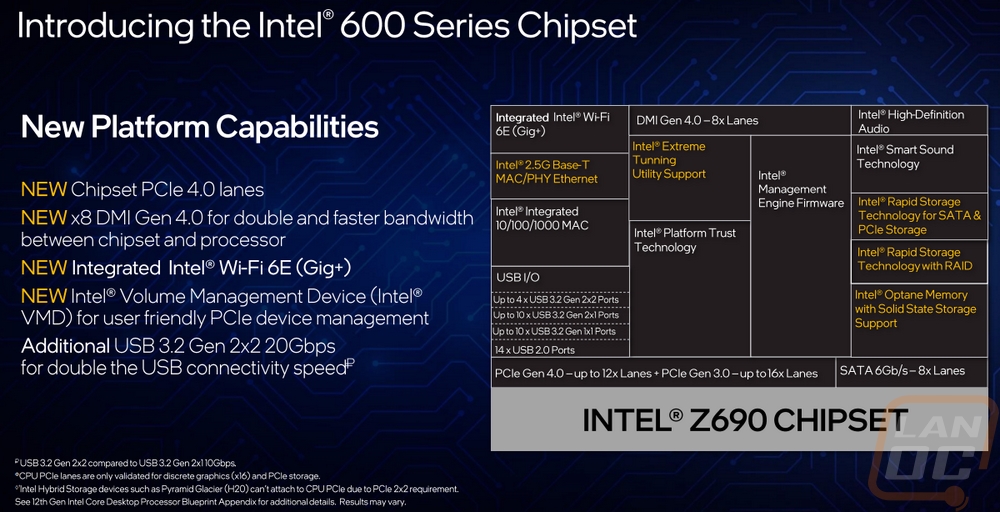
As for the new chipset, the 12th Gen CPUs require new 600 series chipset motherboards. For the performance-focused CPUs like the i9-12900K and the i5-12600K they have the Z690 which is Intel’s new flagship chipset and along with the new LGA 1700 socket to support the 12th generation CPUs. The biggest change is the addition of PCIe 5.0 lanes for the main x16 PCIe slot or depending on the board for two x8 slots directly to the CPU as well as support for an x4 slot at PCIe 4.0 on top of that. The chipset then supports up to 12 PCIe 4.0 lanes and up to 16 PCIe 3.0 lanes on top of that. SATA support is still at 8 SATA ports which given the move to M.2 is more than enough. The connection between the CPU and the chipset has gotten a big upgrade going up to x8 DMI Gen 4.0 for twice the bandwidth. They have also added more USB 3.2 Gen 2x2 ports with support for the ultra-fast connection up to four ports now. The NIC is still the same Intel 2.5G but they have moved the wireless connection up to WiFi 6E from WiFi 6, but you will need windows 11 for that as well as an access point or router that supports it.
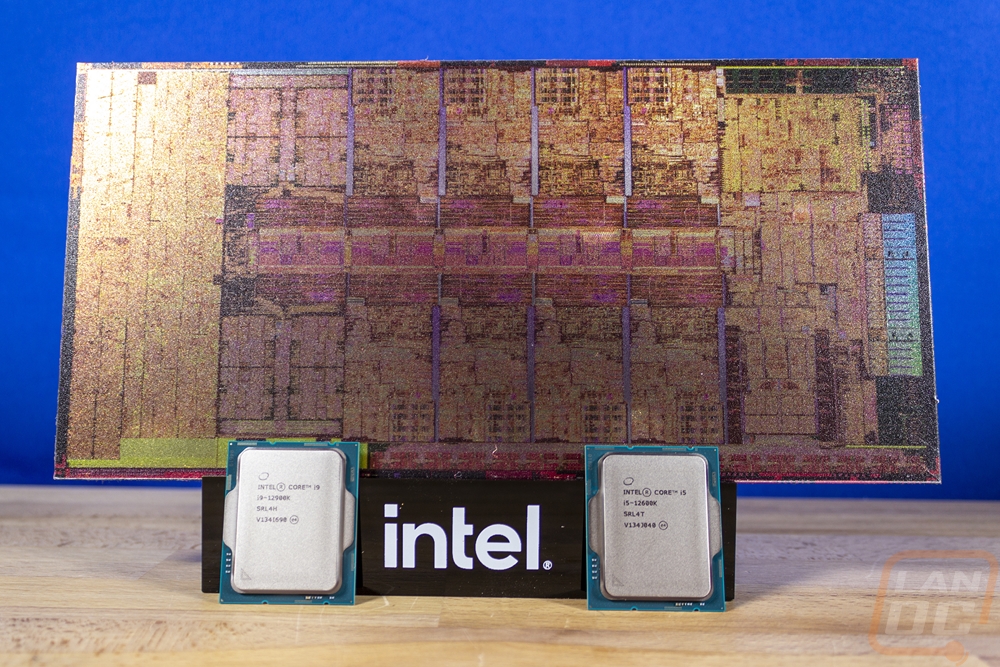
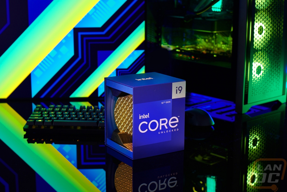
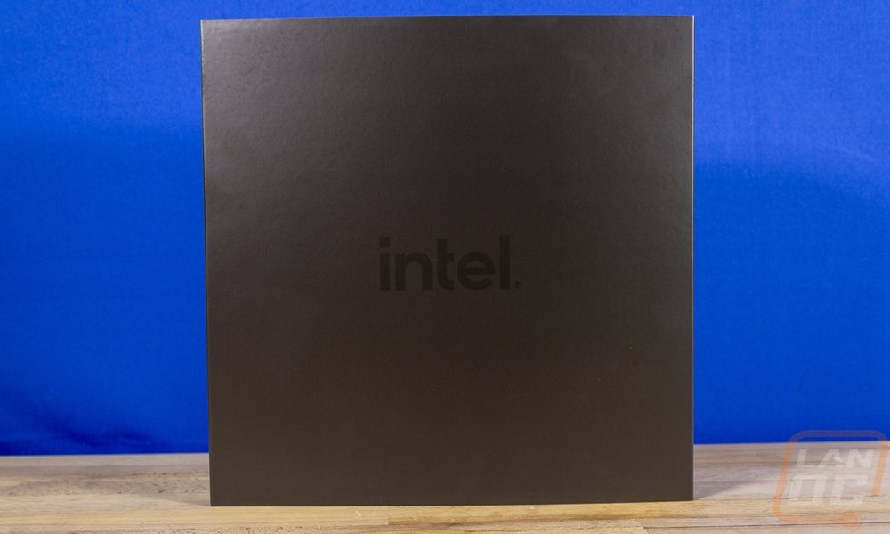
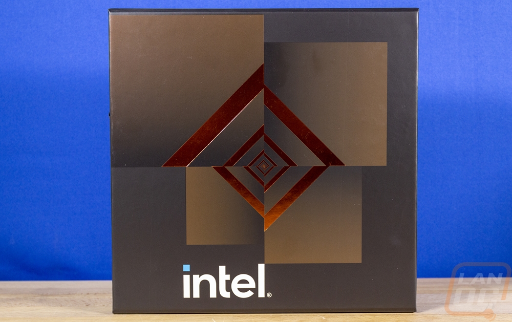
Before getting into testing, I did want to show what the new LGA Socketed CPUs look like and also take a look at the press kit that Intel sent over. They didn’t send the standard packaging although I wouldn’t mind getting that because the new packaging does look good. They take advantage of the multiple blues that Intel uses on the front of the box. There isn’t a crazy looking acrylic design like in the past. But the new packaging does have a gold replica of a wafer of CPU dies inside.
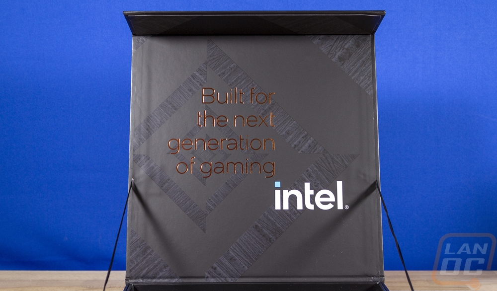
So here is the kit Intel did send over and while the box doesn’t have the same bright blues of the retail packaging the design on the main box under the black cover is sharp. They have the same design on the inside of the box as well only with a black on black that is less visible and the words “Built for the next generation of gaming” with the Intel logo on the underside of the door that opens up.
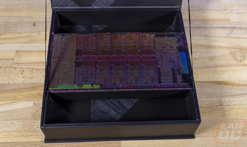
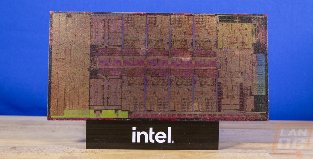
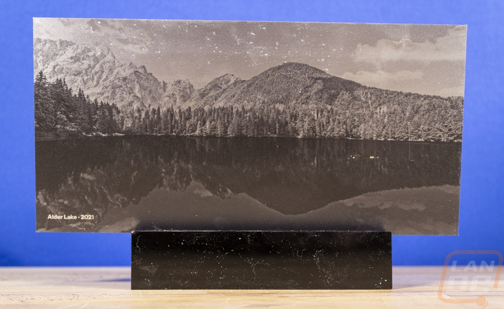
Then when you get inside they have a large panel with an enlarged picture of the Adler Lake die. Under that is also a black stand. The back of the panel also has a picture of the actual Adler Lake as well which is a reservoir in the state of Washington south of the Seattle area. Getting the panel to fit in the stand is tough, the prints on each side of the panel add enough to the thickness that it's almost impossible to fit. But I do like the design.
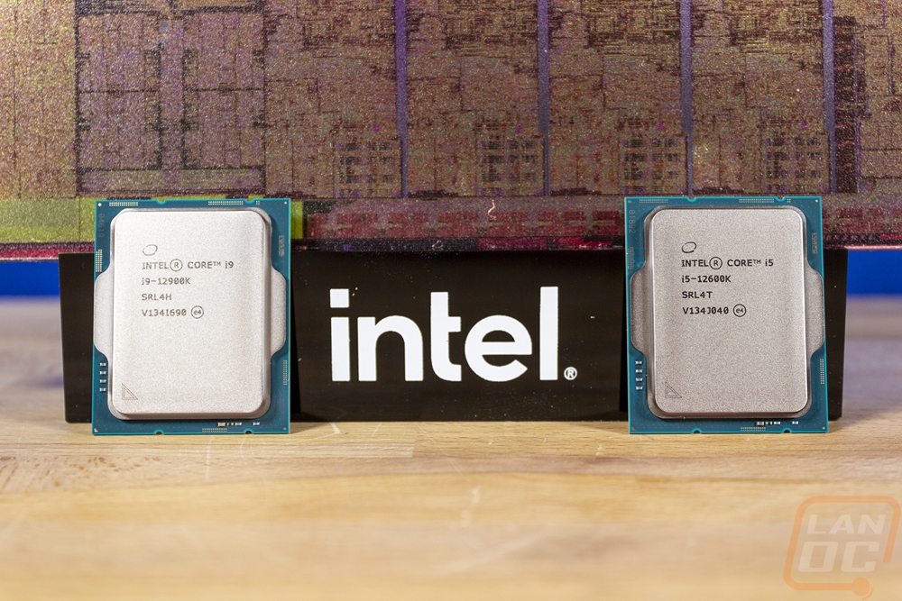
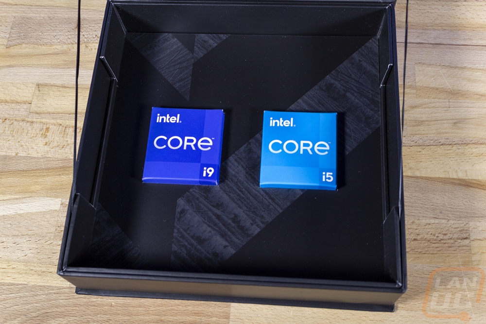
Up under the display then they have two small boxes with the Core i9 and Core i5 branding on them. These are similar to past press kits and both have the CPUs inside with their standard clear plastic clamshell. The new socket size does mean that the clamshells have changed up as well.
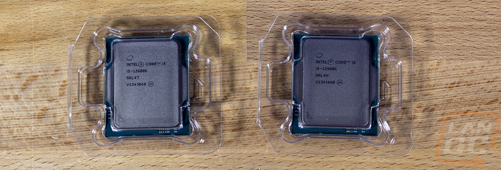
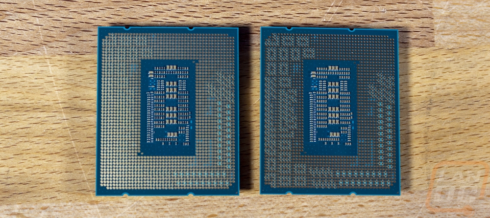
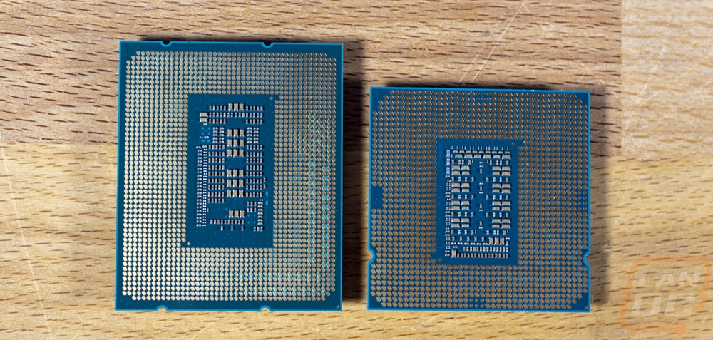
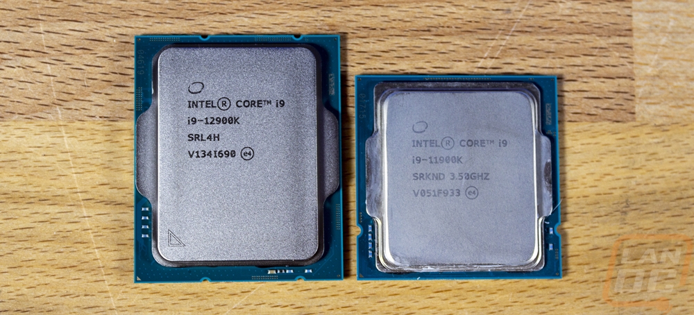
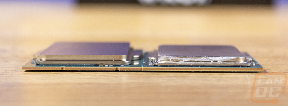
The new CPUs are noticeably different in shape. Intel’s mainstream CPUs have had the same size and shape and shared the same 75mm mounting holes for their heatsinks going all the way back to 2009 and really even the 775 was similar as well only a little smaller. So the move to a rectangle shape which we have mostly only seen with a few larger server sockets. But the shape does make sense, the CPU dies have had a rectangle shape for a long time now, and going with a larger socket has been needed basically from the move to more than 4 cores on the mainstream CPUs. The LGA 1700 is able to get much needed additional connections to help add more bandwidth to the chipset, direct PCIe lanes, and DDR5 as well. On top of that, the larger heatspreader size also means more contact area for coolers to help keep things cool. It also means that past heatsink and AIO designs may not work in some cases and they all do need brackets to support the slightly larger 78mm hole distance which is up from 75mm. You can see the size difference when you put the last generation i9-11900K next to them.