Well as you can tell we are a little late on this article. Last week AMD launched their new CPUs with Vega graphics. Without getting too much into it right now (I’ll explain later) but I spent well over a week fighting with issues when trying to test and I didn’t get things worked out until just before this past weekend. Anyhow, testing is done, now we just need to talk a little about what AMD is doing with these new CPUs and then dive into the results! So let's go see what AMD's new Raven Ridge CPUs are all about!
Product Names: AMD Ryzen 5 2400G and Ryzen 3 2200G
Review Sample Provided by: AMD
Written by: Wes Compton
Pictures by: Wes Compton
Amazon Affiliate Links: Ryzen 5 2400G and Ryzen 3 2200G
Ryzen with Vega Graphics
So the original plan, like our past launch CPU reviews was to dive into every detail of Raven Ridge but honestly, at this point, I think most of you have a decent idea of what it is. So today we are going to keep things a little shorter so we can get into the performance testing that most of you are wanting to see.
Last year with the Ryzen launch it was a huge launch for AMD not just because of the implications at that moment with them in most ways catching up to Intel on the CPU market. Ryzen and the Zen architecture as a whole is a big investment in AMD's future because of their Infinity Fabric design that allowed AMD to be able to shrink and expand the number of cores. Threadripper was a great example of that. Well, the other half of that coin is being able to customize their architecture for APUs and for video game consoles as well. While the Vega launch wasn’t without its issues, hell you still can’t find them. But when you put the two launches together you now have really interesting potential in both the APU and integrated console market.
So a Scalable APU, especially one with Zen and Vega behind it is really interesting because to date most CPUs with onboard graphics leave a lot to be desired when it comes to gaming performance. With Raven Ridge, AMD decided to make some core changes to things to try to realign it to work with both desktop and mobile applications. This meant shrinking the die size down by cutting L3 cache down to 4MB from 8MB and also cutting back on the number of GPU PCI lanes from x16 to x8. To compensate they did bump up clock speeds though. For comparison, the 2400G is similar to the Ryzen 5 1400 but the 2400G has a base clock of 3.6 GHz and a Boost Clock of 3.9 GHz vs 3.2 and 3.45 GHz on the 1400. The PCI lanes change was a cost-saving one as was the move to TIM over soldering under the heat spreader. overclockers and enthusiasts aren’t going to love this change, but officially these are mid-range CPUs and word is AMD isn’t planning on doing this on their higher end CPUs when they get refreshed.
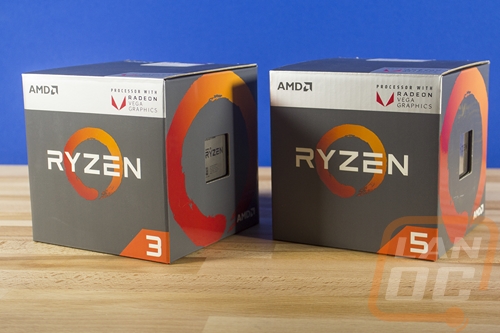
So AMD sent us both the Ryzen 5 2400G and the Ryzen 3 2200G so to take a quick look at the differences. They both have the same 4 core 8 thread configuration and really the base clock speeds aren’t that far apart (3.6 vs 3.5). The 2400G has a little more on the boost clock (.2 GHz) but the main difference is in the onboard graphics. The 2400G has 11 Vega CUs where the 2200G has 8 and the 2400G has a higher clock speed as well. Then from there, they both have the same TDP and Cache and they also now support up to 2933 MHz DDR4 before it is considered overclocking and we learned last year just how much Ryzen likes fast memory. The biggest difference though is in the pricing. The 2200G comes in at $99 where the 2400G is $169, I will have to wait to see the performance before I judge if that is justified or not though.
|
|
AMD Ryzen™ 5 2400G |
AMD Ryzen™ 3 2200G |
|
CPU Cores |
4 Cores, 8 Threads (1 CCX) |
4 Cores, 8 Threads (1 CCX) |
|
CPU Base Clock |
3.6GHz |
3.5GHz |
|
CPU Max Boost Clock |
Up to 3.9GHz |
Up to 3.7GHz |
|
GPU Cores |
11 Radeon™ Vega CUs |
8 Radeon™ Vega CUs |
|
GPU Clock |
Up to 1250MHz |
Up to 1100MHz |
|
L1 Cache |
64K I$, 32K D$ per core |
64K I$, 32K D$ per core |
|
L2 Cache |
512K per core |
512K per core |
|
L3 Cache |
4MB Shared |
4MB Shared |
|
TDP |
65W |
65W |
|
DRAM Supported |
Up to DDR4-2933 (Dual Channel) |
Up to DDR4-2933 (Dual Channel) |
|
Transistors and Die Size |
209.78mm2 / ~4.94 billion |
209.78mm2 / ~4.94 billion |
|
GPU Max Clock |
Up to 1250MHz |
Up to 1100MHz |
|
“Vega” Graphics Cores |
11 Compute Units (704 ALUs) |
8 Compute Units (512 ALUs) |
|
TMUs |
44 |
32 |
|
ROPs |
16 (32-bit) |
16 (32-bit) |
|
FP32 Graphics TFLOPS |
1.76 |
1.126 |
|
FP16 Graphics TFLOPS |
3.52 |
2.252 |
|
MSRP |
$169 |
$99 |