Just to put things in perspective, the GTX 1080 launched May 27th, 2016, that was the last consumer launch of a new series of cards and microarchitecture from Nvidia. That is nearly two and a half years ago. In that time the US elected a new president, we saw a total eclipse over the US, the Cubs broke their 108-year long curse and won the world series, we have even been through TWO Olympics, and not to mention the whole crypto craze! Even crazier, the PC market has completely changed as well, The Intel i7-6700K was the top dog in the consumer market with its 4 cores and the bleeding edge was the recently introduced i7-6950X with its 10 cores. Now 6 and 8 core CPUs are the norm in the mainstream lineups and AMD has the 2990WX with 32 cores on the high end! So even with the 1080Ti and later the 1070Ti, we are long overdue for big graphics launches and Nvidia is going all out. Today both the RTX 2080 Ti and RTX 2080 launch, I’m going to check out the 2080 Ti first and dive into the new Turing architecture, the use for RTX over GTX, the completely new cooler, and of course performance so hang on we have a lot to get through and a short time to get there (RIP Bandit).
Product Name: Nvidia RTX 2080 Ti Founders Edition
Review Sample Provided by: Nvidia
Written by: Wes Compton
Pictures by: Wes Compton
Amazon Affiliate Link: HERE
Turing, RTX, Ray Tracing, what is all of this stuff?
So if you haven’t been following things the last month or so you might have missed Nvidia’s announcement of the new cards and with that one of the most glaring changes. In fact, if that is the case you might even think I had a typo in the title of this article. Typos do happen, especially for me. But no the RTX before the 2080 Ti is real, they did change from GTX to RTX. The reason for this was with the new architecture Nvidia has been focusing on real-time Ray Tracing, the holy grail of gaming. For years now (it goes back to the 70’s even) ray tracing has been used in special effects rending to get the right lighting effects. But up until now, video games could only use multiple effects to try to fake the same look. Ray tracing is at its core, rendering out what each ray of light does including bouncing off of reflective surfaces. This takes a lot of power to figure out and in some cases pixels on the screen might be hit by multiple light rays, compounding the issue and the work needed to do that.
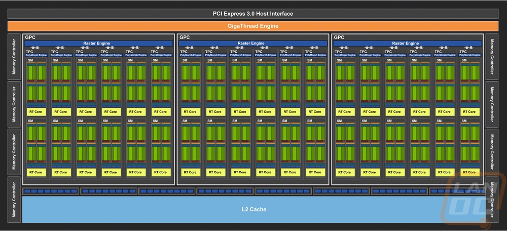
So how do the new cards handle Ray Tracing? Well, first I need to mention the architecture itself. We are finally moving away from Pascal, the architecture used in the 10 series cards. The new architecture is called Turing, a nice nod to Alan Turing who played huge roles in theoretical computer science and an early part in AI. Nvidia built-in ray tracing all the way down into each of their SM’s. That is their Streaming Multiprocessors, each GPU has a specific number of SMs, this determines the GPU size in addition to things like the L2 cache, memory controllers, and their GigaThread Engine. Below I have a picture of a Turing SM and you can see there is one RT core or ray tracing core for each SM. Along with that, each SM has four INT32 cores, four FP32 cores, and four Tensor cores.
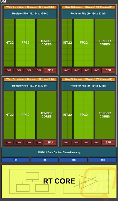
The INT32 and FP32 cores are your normal shaders, but the Tensor Cores are new and interesting. These are focused on deep learning and to go with them Nvidia has also developed DLSS (Deep Leaning Super-Sampling). These “leverage a neural network to extract multidimensional features of the rendered scene and intelligently combine details from multiple frames to construct a high-quality final image”. This allows them to use half of the samples when rendering and to use the deep learning AI to fill in details, giving you similar quality at a much better performance.
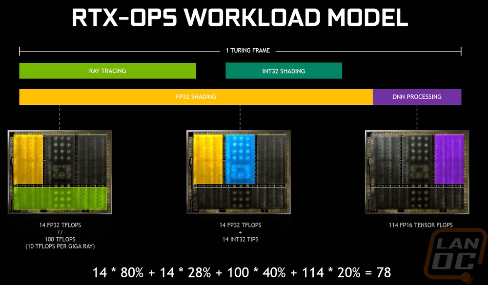
They have also switched over from GDDR5X to the new GDDR6 and that memory is running at 14 Gbps, significantly higher than the 11Gbps of the 1080 Ti and later the upgraded 1080 as well. So what is interesting about this new architecture is it is going in a different direction from the last few from Nvidia. In the past, they have focused on cutting out what isn’t needed for gaming like the asynchronous compute performance. An area that AMD has dominated. But with DX12 taking advantage of asynchronous compute, we now have the INT32 and FP32 cores back together. This new direction has lead to an architecture that isn’t focused on just one thing, opening up the potential for big jumps in performance as game developers take advantage. You see, in the past everything basically ran through the shaders, but now with the Tensor Cores and the RT Cores games can actually run their AI independently of everything else on the Tensor Cores and have their real-time ray tracing as well with the RT cores. The image below shows what I mean.
Okay, what about the new cards? Well, there are currently two cards out today, with the RTX 2070 coming out in October. What is interesting though is at least currently they don’t replace the previous models, in fact, there isn’t any indication yet that the GTX lineup is going away. Both the RTX 2080 Ti and the RTX 2080 are priced above the GTX 1080 Ti. Is Nvidia pushing to create a new level of high end? Maybe, I’m not really sure. But let's look at the specs. When just looking at CUDA cores we can see that the 2080 Ti is with its TU102 GPU is much larger than the 1080 Ti, same with the number of texture units though they have the same number of ROPs. Clock speeds for the 1080 Ti range from the core speed of 1350MHz and up to the boost clock of 1635Mhz, this is both lower and higher than the 1080 Ti. The RTX 2080, like the 10 series cards is clocked higher than the Ti model but the Ti makes up for the lower clock speeds with significantly more CUDA cores. The 2080 Ti also has more VRAM and a wider pipe with its 352-bit memory bus over the 256-bit memory bus of the 2080. This is similar to the 1080 Ti and the 1080, in fact, they both have the same amount of memory as well (11GB and 8GB).
The Turing GPUs are now made at 12nm using the same FinFET process as Pascal. But even with that smaller process, the die sizes are crazy, the TU102 is 754 mm squared, this is the second largest GPU die ever made and over twice the size of the GTX 1080. The 18.6B transistors take up a little space. The RTX 2080 is a low lower with 13.6B transistors but still above the 12B of the GTX 1080 Ti and nearly double the 7.2B of the original GTX 1080.
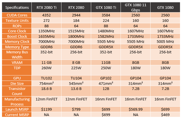
All of that does need a lot of power to push, even with the smaller manufacturing process. The RTX 2080 comes in at 260 watts, this is higher than Nvidia’s single cards in the past. The GTX 690, their dual GPU card did have a TDP of 300. The RTX 2080 is much better with a 225-watt TDP. The price is the other big factor with these cards. As I mentioned they don’t really push the 10 Series cards out. The RTX 2080 Founders Edition comes in at $799, Nvidia says aftermarket cards may come in at $699, but as we have seen in the past normally having the Founders Edition or reference cards priced higher lead to other cards matching or going higher. The GTX 1080 Ti launched at $699 and that is where the price is as well, pricing is only now calming down from the crypto craze. The RTX 2080 Ti is even higher with its Founders Edition pricing set to $1199, blasting past the 1k price point. The starting price for aftermarket 2080 Ti’s is $999, but again we will have to wait to see if cards come in at those prices.
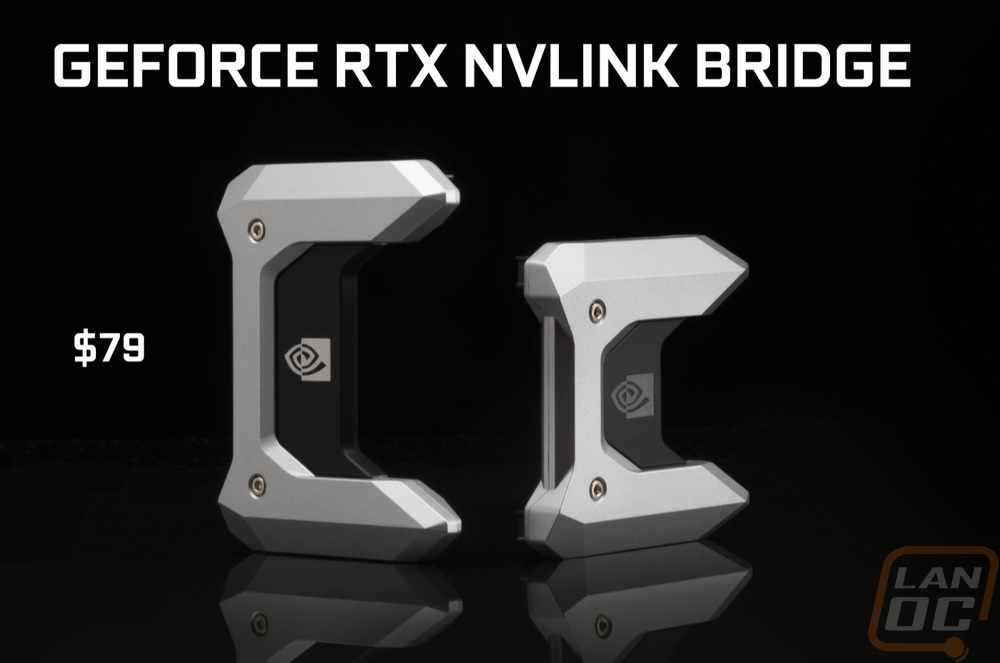
Also announced was the RTX NVLink, a replacement for the SLI bridge. With the HB SLI bridges just coming out with the 10 series cards it is disappointing to see them go away in favor of the NVLink. The NVLink isn’t really new, Nvidia has been using it on their server cards for a while now. But there are a few things to note about it. For starters, it will run you $79, so it is more expensive than the HB SLI bridges. It will also only work with the RTX 2080 and RTX 2080 Ti, the also announced RTX 2070 does not support it. So in addition to seeing multi-card configurations die for the x60 cards a while back, it has now also gone away for x70 cards. I’ve also heard that they will not be included with motherboards like HB SLI bridges have been. Aftermarket versions will be available, but they will be rebranded versions of the Nvidia bridge pictured below and at the same price.
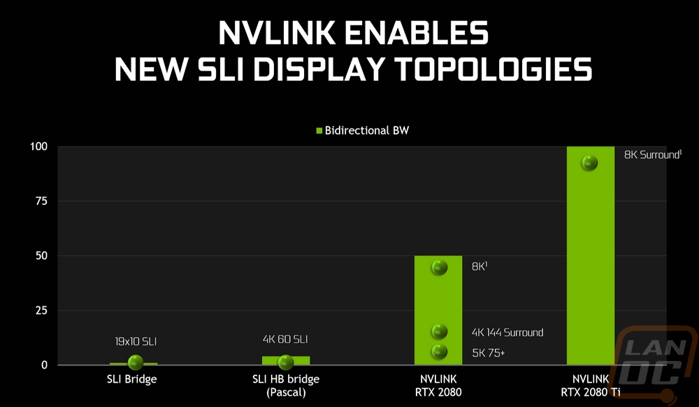
The new bridges do offer a LOT more bandwidth. Nvidia included this slide in their presentation showing the difference. Sadly there wasn’t any scale on the graph. Diving into the whitepaper shows that the numbers are in GB/second bidirectional bandwidth. Allowing for 4k144Hz and 8K surround bandwidths. Each link offers 25 GB/s each direction, the TU102 has two and the TU104 has one. All of this means you can now hook up more monitors to different GPUs and there is bandwidth to send the frames over to the video card.
Nvidia has also brought on board new overclocking features. For starters, GPU Boost is now in its 4.0 variation. The biggest change here is now the profiles are user editable, allowing you to push the limits more as needed. But the biggest introduction in this area is Nvidia Scanner, a built-in overclocking option that spends up to 20 minutes testing and retesting to put together the ideal profile. Auto overclocking isn’t really new, but this is an improvement on what has been done in the past. It goes as far as testing different voltage points and then interpolating between them and testing over and over with a mathematical algorithm that checks for failures while testing to find the limits without hard crashes.
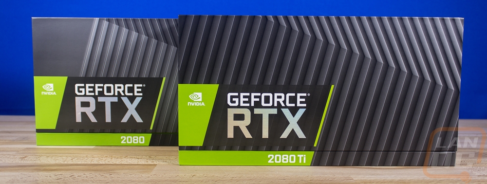
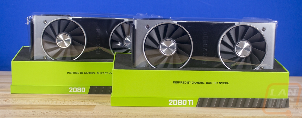
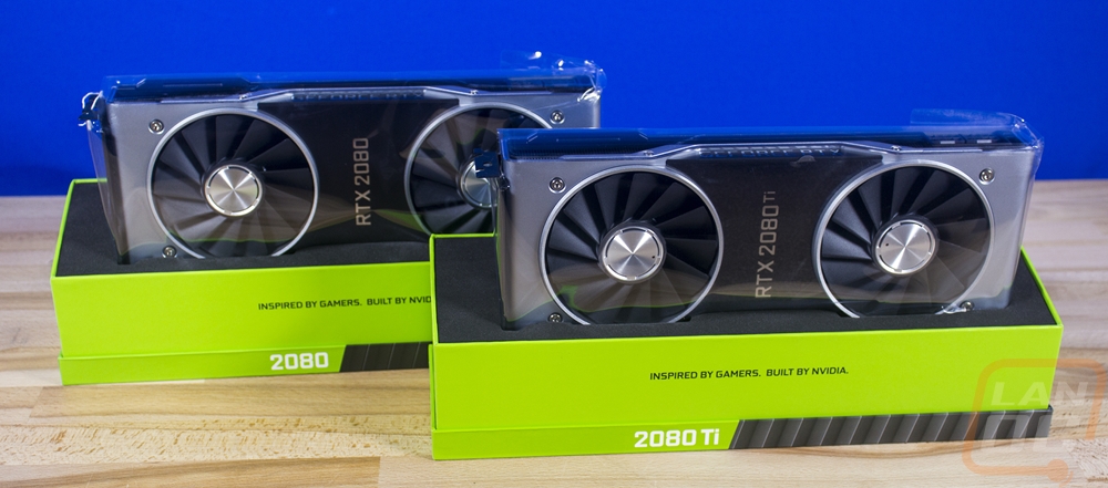
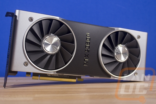
The new cards have also made big changes in their overall look as well. I’ll include these teaser pictures, but I will dive into the cooler in the card layout section.