It’s hard to believe that Nvidia’s Kepler architecture has been around for nearly two years now. In those two years Nvidia has continued to innovate with Kepler exclusive features like Shadowplay and PC streaming to your Nvidia Shield. Well now it is finally time to take a look at what Nvidia has been working on with its latest architecture, Maxwell. Interestingly enough Nvidia isn’t launching their new architecture with a flagship card, they chose to fill in a gap in their current 700 series of cards down at budget price points. Today they are introducing the GTX 750 Ti and the GTX 750 and I will be putting a GTX 750 Ti through its paces as well.
Product Name: Nvidia GTX 750 Ti
Review Sample Provided by: Nvidia
Written by: Wes
Pictures by: Wes
Maxwell and more
The launch of a budget card wouldn’t normally get the attention of a lot of people. But something tells me this one will be a little different. With this being the first peak at Maxwell it will be interesting to see how well it performs. As with any architecture change Nvidia worked on improving performance from Kepler to Maxwell but what is more interesting is their focus on lowering power usage. This was a big focus going from Fermi previously to Kepler as well and it paid off very well by leaving them a lot of room on the high end to increase clock speeds to bring out newer and faster video cards. Lower power consumption also allows for packing more power into smaller form factors, like the shorter PCBs seen on a few Kepler cards. In our documentation on Maxwell Nvidia is claiming an improvement of twice the performance per watt over Kepler while using the same 28nm manufacturing process.
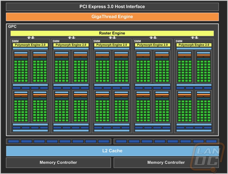
So what is Maxwell all about? Well first generation Maxwell GPUs have the same API functionality as Kepler GPUs and a lot of the fundamentals are the same on the GPU as well. Maxwell uses multiple SM units within a Graphics Processing Cluster (GPC) and each SM includes a polymorph engine and texture units. ROPs are still aligned with L2 cache slices and memory controllers, but they have greatly increased the L2 cache size.
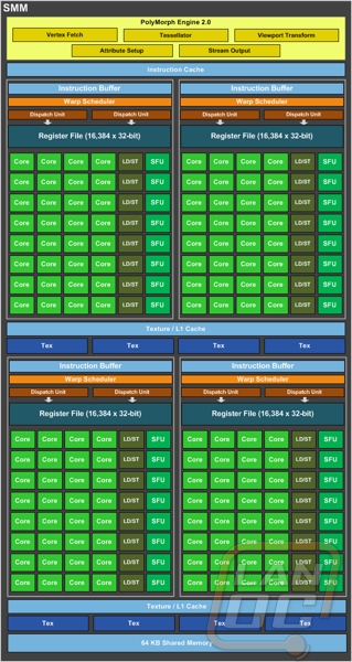
One of things they did to speed things up was to rewrite the SM scheduler architecture and algorithms to avoid unnecessary stalls while further reducing the energy per instruction required for scheduling. They also simplified the SM design to save area and power as well the side benefit of a lower computation latency. Each Maxwell SM is significantly smaller while still delivering 90% of the performance of a Kepler SM. That smaller size allowed them to pack in more SMs, on the GK107 they had two where the GM107 (Maxwell) has 5, increasing the number of CUDA cores by 1.7 times and giving 2.3 times more performance in shader performance.
Here is a direct comparison between the older GK107 to the new GM107 introduced today.
|
GPU |
GK107 (Kepler) |
GM107 (Maxwell) |
|
CUDA Cores |
384 |
640 |
|
Base Clock |
1058 MHz |
1020 MHz |
|
GPU Boost Clock |
N/A |
1085 MHZ |
|
GFLOPs |
812.5 |
1305.5 |
|
Texture Units |
32 |
40 |
|
Texture fill-rate |
33.9 Gigatexels/sec |
40.8 Gigatexels/sec |
|
Memory Clock |
5000 MHz |
5400 MHz |
|
Memory Bandwidth |
80 GB/sec |
86.4 GB/sec |
|
ROPs |
16 |
16 |
|
L2 Cache Size |
256KB |
2048KB |
|
TDP |
64W |
60W |
|
Transistors |
1.3 Billion |
1.87 Billion |
|
Die Size |
118 mm |
148 mm |
|
Manufacturing Process |
28-nm |
28-nm |
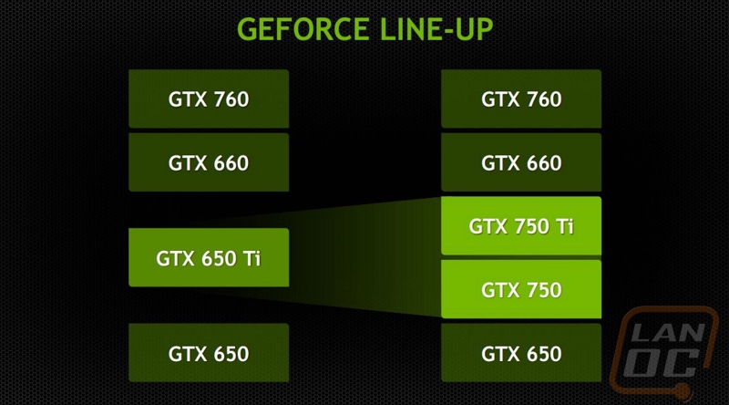
So what does the addition of these new cards do to Nvidia’s product lineup? Well as you can see below the GTX 750 Ti and GTX 750 slip in under the GTX 660 and above the GTX 650, replacing the GTX 650 Ti. It’s still a little confusing with the mix of 600 and 700 series cards though. I’m not sure if I would prefer it this way over rebranding cards just to fill in those blanks. Both options can be confusing.
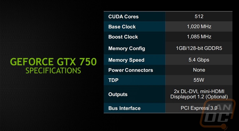
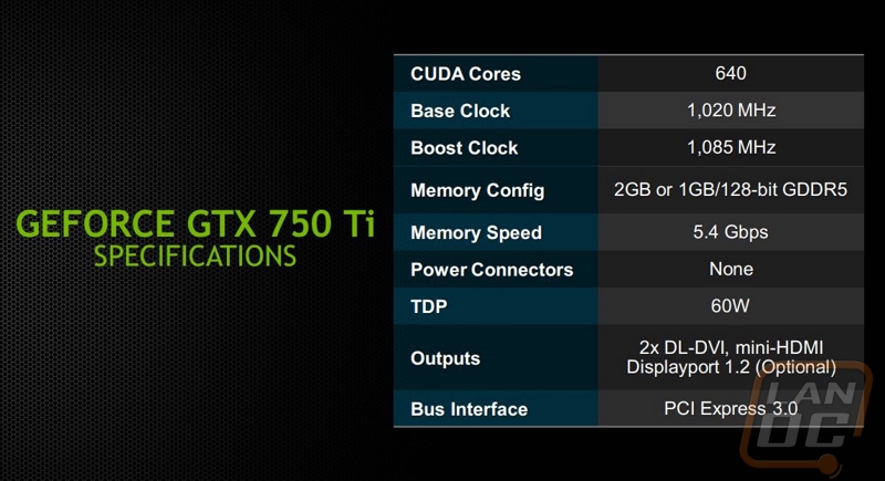
So here is a peak at the specifications of the GTX 750 Ti and the GTX 750, both being introduced today. They both are based on a new GM107 Maxwell GPU. They share similar clock speeds but the Ti will get you a few more CUDA cores. Additionally the Ti pulls a little more wattage at 60 watts, but even so that is less than the Kepler cards it is replacing. The price breakdown is as follows
GTX 750 Ti 2GB : $149
GTX 750 Ti 1GB : $139
GTX 750 : $119
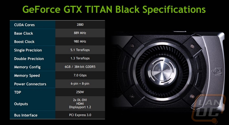
The third card introduced today is the often rumored GTX Titan Black. Nvidia bumped up the number of CUDA cores from 2688 to 2880, improved the clock speed both on the GPU as well as the memory to improve the Single Precision performance from 4.5 Teraflops to 5.1 Teraflops. Sadly we don’t have a card on hand to test, but the improvements seem to be focused on bringing the Titan up to the GTX 780 Ti levels of performance while still keeping the double precision performance that makes the Titan such a monster. The price point is staying at the $1,000 mark that the original Titan has held as well.