 The PC world is always moving, innovating, and reinventing itself. Every day, every month, and every year we see new products introduced from every aspect of the industry. You will almost never will you see any of those new products cause more than just a small hiccup in the overall scheme. There is one company that is a little different. When we come across a main Intel launch everyone in the industry stops what they are doing to make sure they are aligned with what Intel is doing. Today I can finally talk to you about Intel’s newest launch, a new socket, chipset, and CPU. Today we are taking a look at the new i7-3960X CPU and the x79 chipset that is introduced along with it.
Product Name: Intel i7-3960X and Intel DX79SI
Review Sample Provided by: Intel, Kingston
Review by: Wes
Pictures by: Wes
What is Sandy Bridge-E and X79
Before we get into that Sandy Bridge-E is all about let me explain Intel’s product cycle. They describe it as a Tick then Tock, like a clock. As they continue to shrink their manufacturing process we will see a “tick” and a “tock” for each shrink. The first of the two the “tick” will just be a more efficient version of the microarchitecture introduced before. A good example of this was the introduction of the Nehalem lineup a few years ago; with the die shrink later creating Westmere. Last year Intel introduced Sandy Bridge and we will see the die shrink to 22nm when they introduce Ivy Bridge.
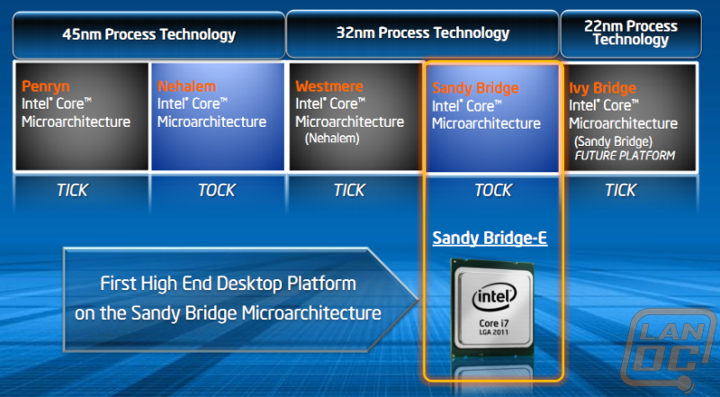
Where it gets a little confusing is the use of two different consumer product lines/sockets the use of the same i7 moniker across them. The two product lines are mainstream and then their high end desktop platform. For the past year the mainstream line was LGA 1155 with Sandy Bridge and the high end desktop line was LGA 1366. LGA 1366 was getting long in the tooth, and this was even more obvious when compairing performance numbers to Sandy Bridge CPU’s. Of course the 6 core variations could hold their own but were still based on an old microarchitecture. That’s where Sandy Bridge-E comes in. Sandy Bridge-E is based on the LGA 2011 socket and uses the Sandy Bridge microarchitecture, with a few very important improvements to be able to support high end performance.
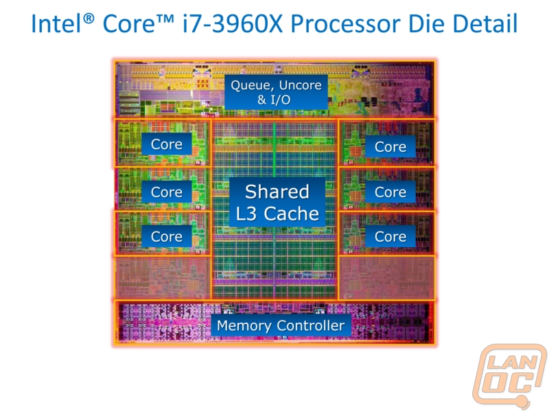
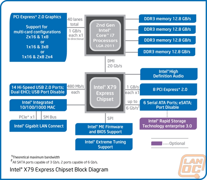
Other than the obvious improvement of 6 cores (also note the two other spots to upgrade to 8 cores in the future), what else was improved? When compared to the LGA 1155 socket Sandy Bridge CPU’s the biggest advantage overall on the Sandy Bridge-E CPU’s is the added bandwidth. The number of PCIe lanes on Sandy Bridge CPU’s was very limited causing motherboard manufactures to get very creative on the high end gaming motherboards. A good example of this would be MSI having to shut off some of the USB 3.0 ports when you are running two or more video cards in SLI. With a total of 16 PCIe Lanes a Sandy Bridge CPU was capped with one x16 video card. Sandy Bridge-E has a total of 40 PCIe Lanes. Giving lots of room for whatever you might need. Although those lanes are not listed as PCIe 3.0 they are capable of 8GT/s, its believed that they will be certified later on. Until then we will just have motherboard manufactures mentioning PCIe 3.0 readiness. On top of all of the PCIe Lanes Intel beefed up the built in memory controller. X58 had triple channel RAM, Sandy Bridge has dual channel, and Sandy Bridge-E has quad channel RAM! The four channels together give you a total of 51.2 GB/s of memory bandwidth.
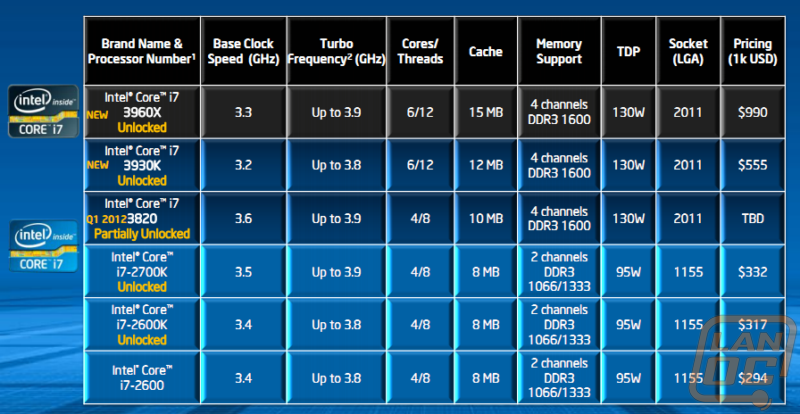
Now although we are reviewing the i7-3960X today, Intel is also introducing a second CPU with a third coming out in Q1 of 2012. I’ve included the family listing blow . The top three CPU’s listed are/will be 2011 socket CPU’s with the bottom three standard 1155 socket Sandy Bridge CPU’s. As far as product names go the Sandy Bridge-E CPU’s will be numbered in the 3k series of numbers with Sandy Bridge in the 2k, and the original Nehalem CPU’s in the sub 1k series. From there you can break them down by the last three numbers and the letter at the end. In this case the 3960X can be broken down by 3-960-X. Calling this a 960 leaves room for more CPU’s in the future with the X at the end designates this as an Extreme series CPU that is unlocked and a flagship CPU. The K seen at the end of the i7-3930K and i7-2700K both also stand for unlocked multipliers, but don’t get the Extreme name because they are not at the top of the Intel CPU foodchain.
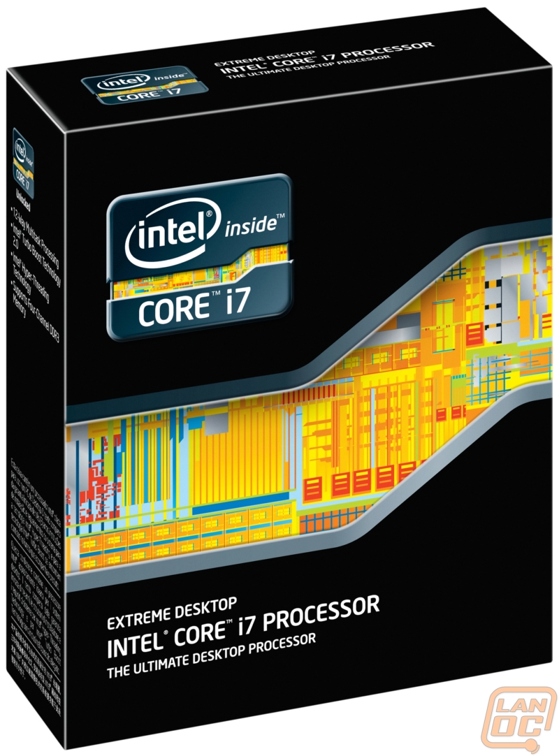
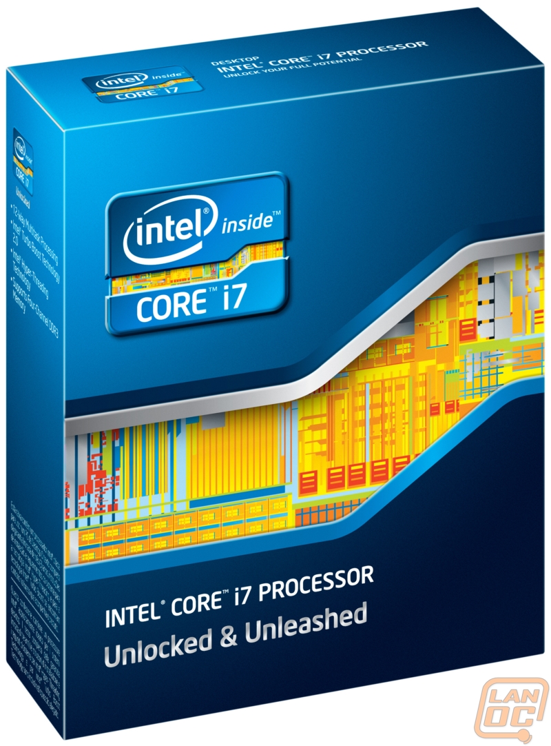
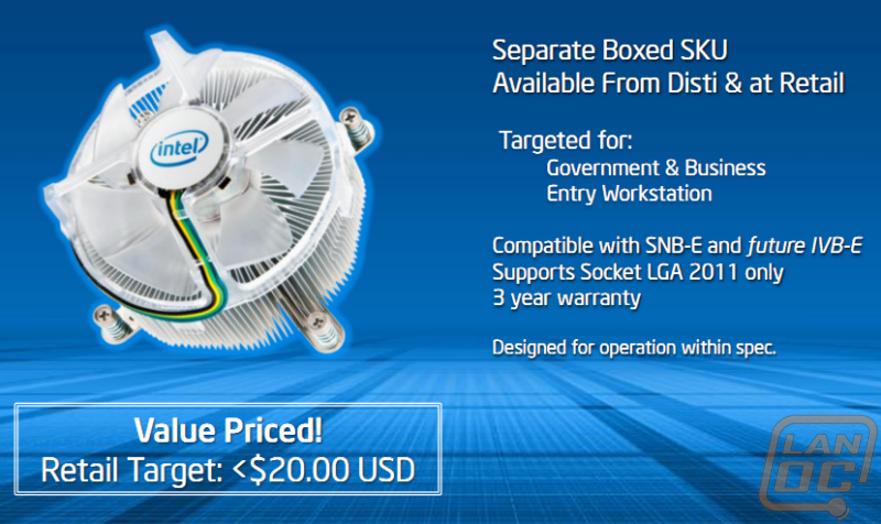
The packaging for Intel’s new CPU’s follows the same design that we have come to expect. But there is one major difference, the size. The new size has to do with another change, no heatsink included. With this being the performance lineup Intel has decided to let you decide on what heatsink to go with rather than force a design on you.
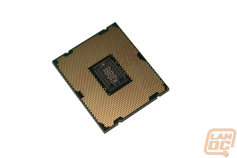
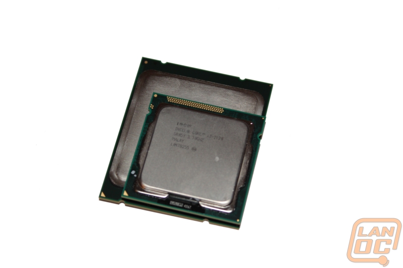
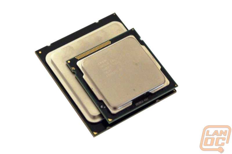
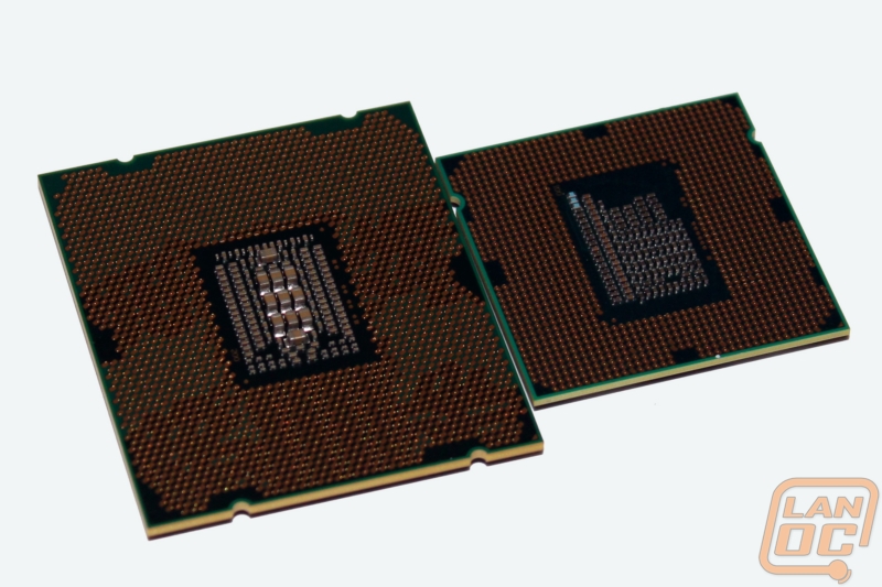
With 2011 pins the size of the new LGA 2011 socket CPU’s is considerably larger than other Sandy Bridge CPU’s. I’ve included a comparison photo of the different between the two below. You can also see a few of the design changes in the heatspreader. Unlike Sandy Bridge the heatspreader has a more defined edge. You will also notice the hole in the heatspreader. With our CPU being an engineering sample don’t know for sure if that will carry on to production CPU’s, but we have seen this in the past. The hole is used to insert the glue needed to attach the heatspreader to the CPU.
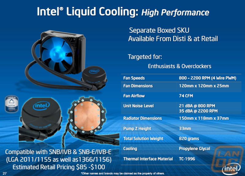
That doesn’t mean they won’t have a cheap heatsink available. They have still developed a standard heatsink for government and business use, you will just have to pick it up along with the CPU. They are also recommending a who list of heatsinks and water cooling solutions from other manufactures to keep your new Sandy Bridge-E cool. They still went ahead and designed their own water cooling solution along with Asetek. I have included the info here, but read more in our cooling section to find out more as we do have one to test.

To go along with the new CPU you have a new chipset, X79. While talking about the new CPU I mentioned the 40 total PCIe Lanes for graphics cards and the quad channel memory. The X79 chipset takes care of everything else on your motherboard. Intel has given a total of 480 Mb/s bandwidth each to a total of 12 USB 2.0 port capability on the X79 chipset. For the network card Intel has integrated one of their very own 10/100/1000 cards along with Intel High Definition Audio. The X79 chipset also runs 8 PCIe x1 slots on top of the direct lanes to the CPU. For SATA ports the base X79 chipset will get you a total of six with two of those ports being SATA 3. Along with that motherboard manufactures will have the option of including Intel’s Rapid Storage Technology for configuring your RAID on the X79 SATA ports.