 You have all seen and heard the rumors for months now about Nvidia’s upcoming GPU code named Kepler. When we got the call that Nvidia was inviting editors out to San Francisco to show us what they have been working on we jumped at the chance to finally put the rumors to rest and see what they really had up their sleeve. Today we can finally tell you all the gory details and dig into the performance of Nvidia’s latest flagship video card. Will it be the fastest single GPU card in the world? We finally find out!
Product Name: Nvidia GTX 680 Kepler
Review Sample Provided by: Nvidia
Review by: Wes
Pictures by: Wes
Kepler what’s it all about

During editors day Nvidia opened things up by boldly stating that the new GTX 680 will be the most powerful and most efficient card on the market. They went on soon after to bring out Mark Rein, Vice President of Epic Games to show off a demo that they made last year called the Unreal Samaritan Demo. Last year when the demo was originally shown they required a three GTX 580 powered rig to show it off. While playing the demo he pointed out that that same demo is now running great on just one card, the Kepler based GTX 680. Obviously the GTX 680 isn’t three times as powerful as a single GTX 580, but throughout the day they went over all of the pieces that fit together to help them realize that performance increase.
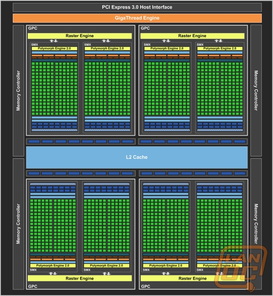
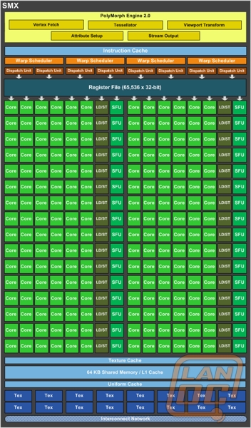
First let’s jump into the hardware itself because that is obviously a big part of the performance increase. At the core of the GTX 580 there were 16 Streaming Multiprocessor’s (SM), each having 32 cores. With the GTX 680 Nvidia has moved to what they are calling the SMX. Each SMX has twice the performance/watt when compared to the GTX 580 and each has 192 cores. Now the GTX 680 has a total of 8 SMX multiprocessor’s making for a total of 1536 Cores!
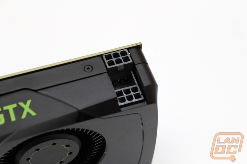
Like I mentioned before they said the GTX 680 would be a very efficient card considering its performance. That was obvious as soon as they posted up its new TDC of 195 Watts, sporting just two six pin connections. For those who are counting that’s 50 watts less than the GTX 580 and around 20 less than the HD 7970.
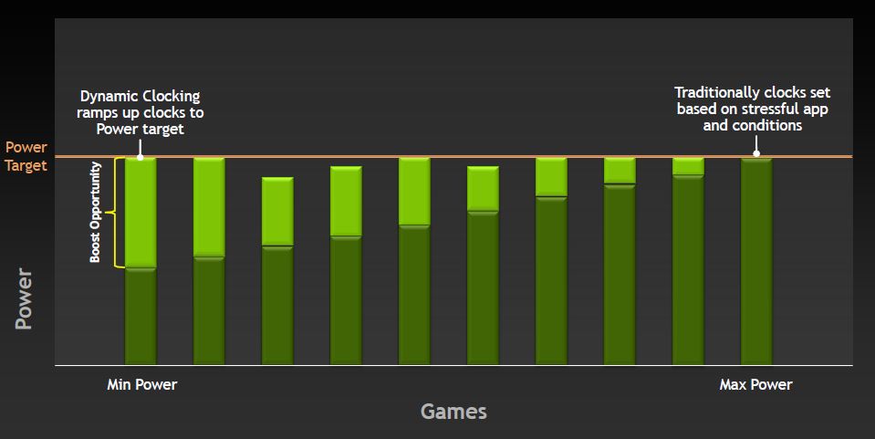
It’s clear that Nvidia took a look at what Intel has been doing on the CPU side of things when creating the GTX 680. Kepler introduces a new Nvidia technology called GPU Boost. This is similar to what Intel’s Turbo mode is, but with a different approach. The idea is that some games end up requiring less actually wattage to compute than other games. In the past they have set their clock speed by the maximum power usage in the worst case application. With GPU boost the GPU is able to notice that its being underutilized and it will boost core clock speed and on a lesser level memory clock speed. You shouldn’t look at this as overclocking, because you can still overclock the GTX on your own. GPU boost runs all of the time no matter what meaning you can’t turn it off, even if you would like to. When you are overclocking in the future you will actually being changing the base clock speed, GPU boost will still be on top of that. For those that are wondering, GPU Boost polls every 100ms to readjust the boost. This means if a game gets to a demanding part you’re not going to have your card crash from pulling too much voltage.
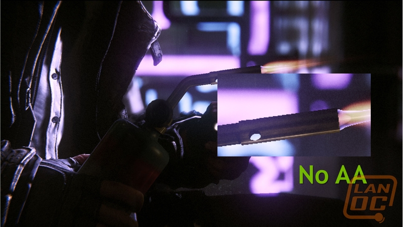
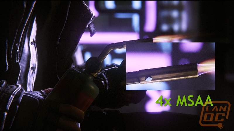
Like I said before, more powerful hardware are only part of the picture when it comes to Unreal’s demo system going from three GTX 580’s to one GTX 680. Nvidia spend a lot of time working on FXAA and their new TXAA Anti-Aliasing techniques. In the demo mentioned they went from using MSAA 4x to FXAA 3. Not only did they see better performance but it actually did a better job smoothing out the image. I’ve included the images below for you guys to see, I think you will agree.

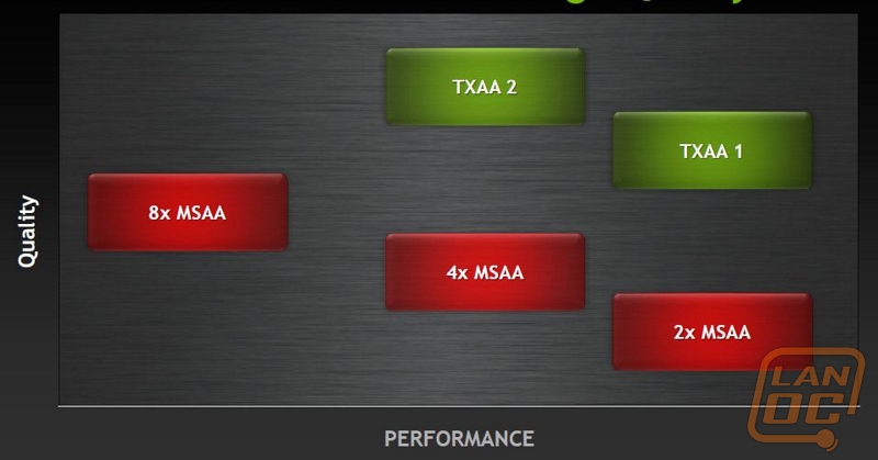
As I mentioned before on top of talking about FXAA Nvidia launched a new Anti-Aliasing called TXAA. TXAA us a mixture of hardware anti-aliasing, custom CG film style AA resolve, and when using TXAA 2 an optional temporal component for better image quality. By taking away some of the traditional hardware anti-aliasing TXAA is able to look better than MSAA while performing better as well. For example TXAA 1 performs like 2x MSAA but looks better than 8xMSAA.


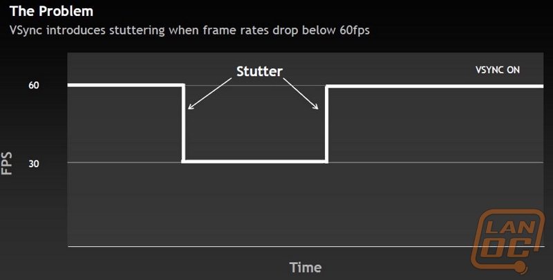
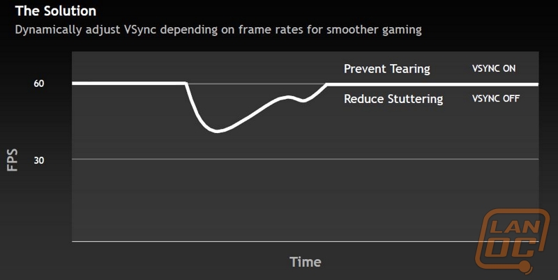
Another feature being implemented with Kepler is one called Adaptive V Sync. This is designed to better your gaming experience. One complaint that people have with high end GPU’s is screen tearing. One way to prevent that is to turn on VSync. But the downside to this is when you drop below 60PFS it will force you to 30FPS, this causes a major hiccup and slowdown when the GPU may be able to actually give you 59 FPS. Adaptive VSync watches for this and turns VSync off whenever you drop below 60 FPS making the transition smoother.
On top of all of those important features that improve your gaming experience there are a few other smaller things introduces also that I would like to quickly go over. First, 2D surround now only requires one GPU to run three monitors. This means you don’t need to run and pick up a second card just to game with three monitors, as far as performance goes, it will still depend on what you’re playing. To go along with this they are also introducing 3+1. This is a setup that allows you to run a fourth monitor above your triple monitors. You can run this while still gaming on the three, this is perfect for watching notifications or TV shows during slow periods of your gaming.
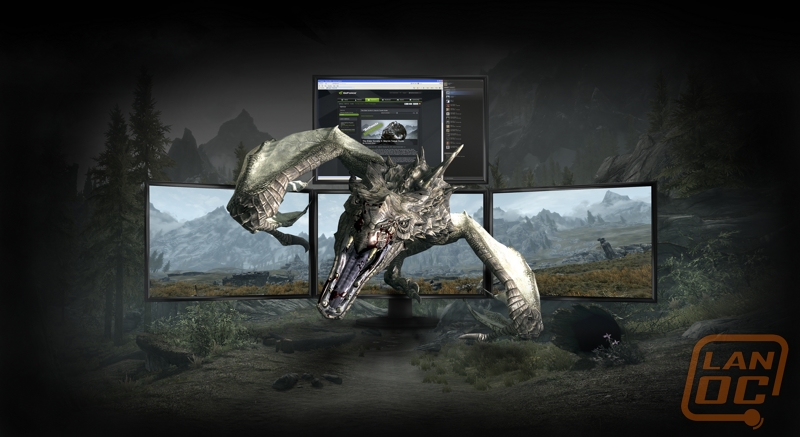
Other surround improvements include finally moving the task bar to the middle monitor, something that should have been done from the start. You can now also maximize windows to a single monitor also. A small tweak added now allows you to turn off the bezel adjustment on the fly when running multiple monitors; this is great if you are running your macros in wow across two monitors for example, you won’t miss out on anything.
Lastly they also have tweaked the GPU’s performance to be a little more optimized when you are running a single monitor game on one of your triple monitors.
Specifications
|
Processing Units |
|
|
Graphics Processing Clusters |
4 |
|
Streaming Multiprocessors |
8 |
|
CUDA Cores |
1536 |
|
Texture Units |
128 |
|
ROP Units |
32 |
|
Clock Speeds |
|
|
Base Clock |
1006 Mhz |
|
Boost Clock |
1058 MHz |
|
Memory Clock (Data Rate) |
6008 MHz |
|
L2 Cache Size |
512KB |
|
Memory |
|
|
Total Video Memory |
2048MB GDDR5 |
|
Memory Interface |
256-bit |
|
Total Memory Bandwidth |
192.26 GB/s |
|
Texture Filtering Rate (bilinear) |
128.8 GigaTexels/sec |
|
Physical & Thermal |
|
|
Fabrication Process |
28 nm |
|
Transistor Count |
3.54 Billion |
|
Connections |
2x DL-DVI HDMI Displayport 1.2 |
|
Form Factor |
Dual Slot |
|
Power Connectors |
6-pin + 6-pin |
|
Recommended Power Supply |
550 Watts |
|
Thermal Design Power (TDP) |
195W |
|
Thermal Threshold |
98 Degrees Celsius |
|
Bus Interface |
PCI Express 3.0 |
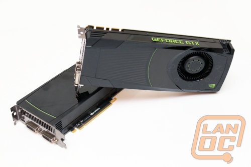
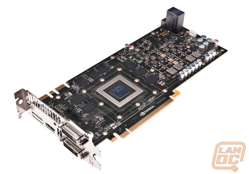
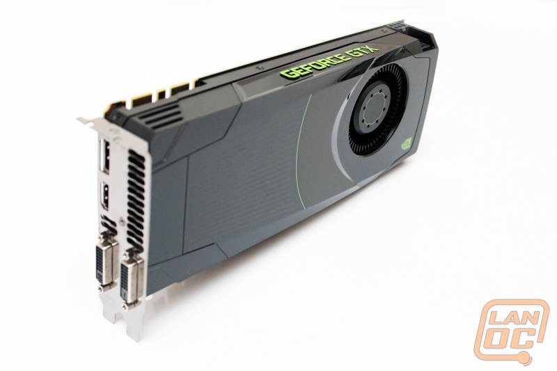
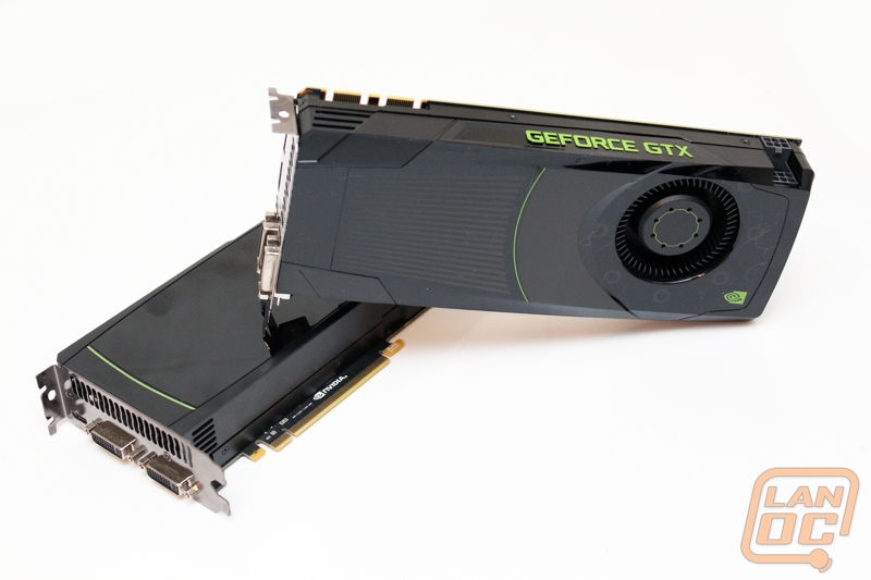
Card Layout and Photos
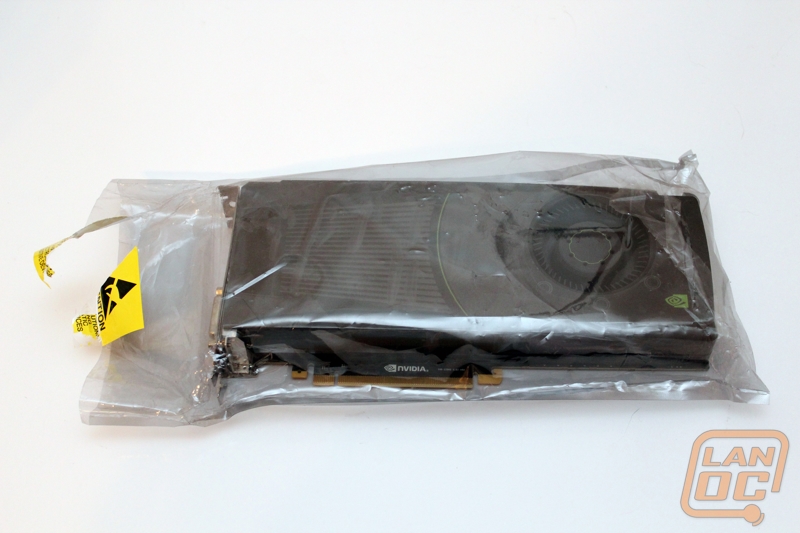
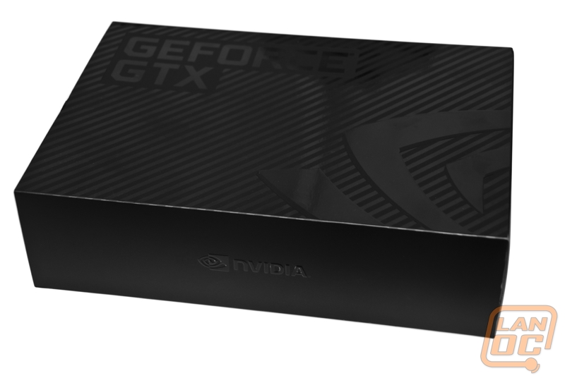
What’s that hiding in its electrostatic bag.. Don’t be shy we won’t hurt you. The GTX 680 actually came to me in the sexy packaging below, but I had to leave it in San Francisco when I left due to limited space in my bags.
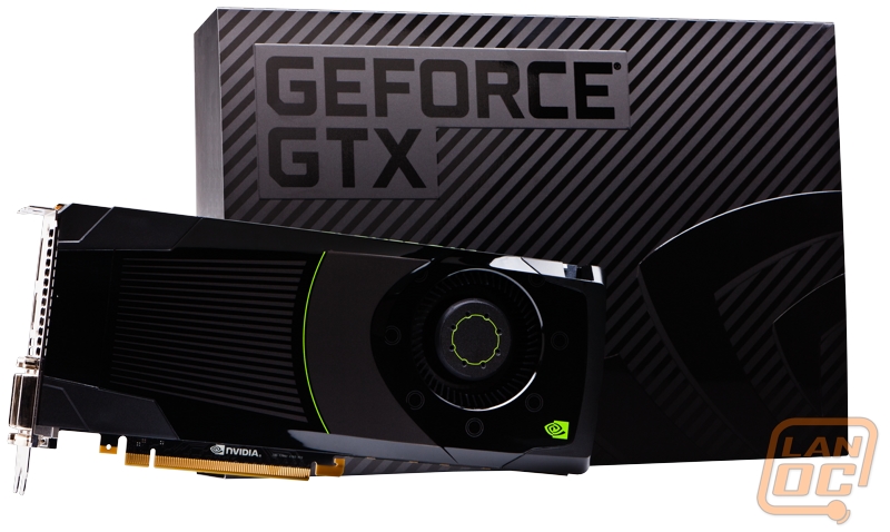
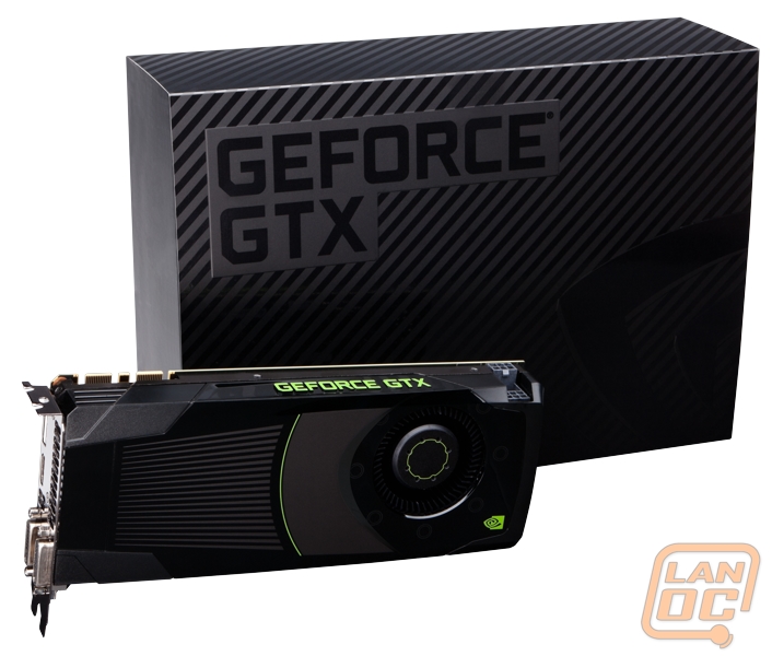
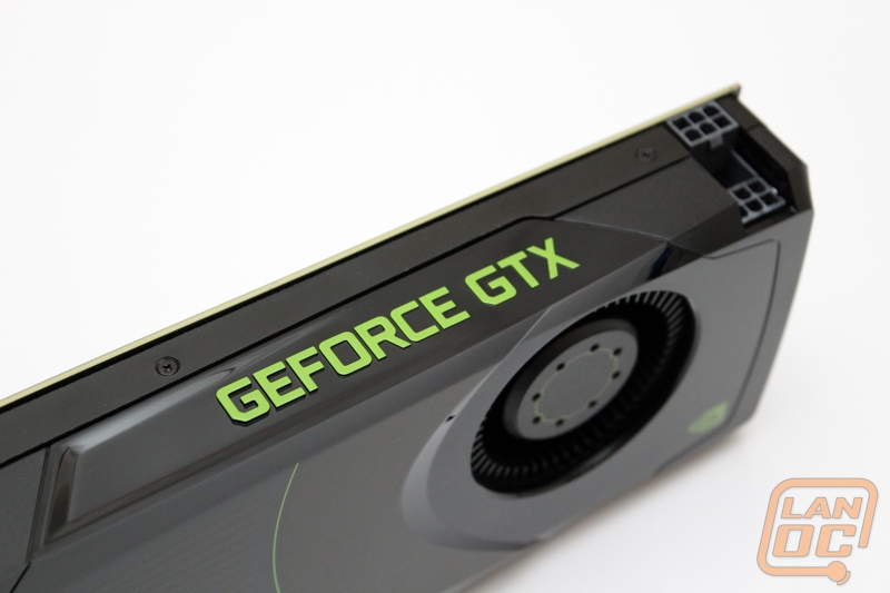
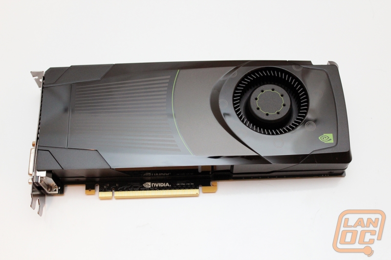
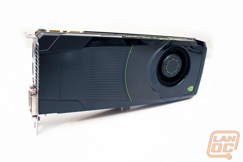
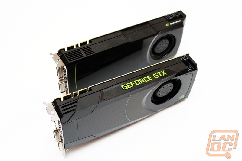
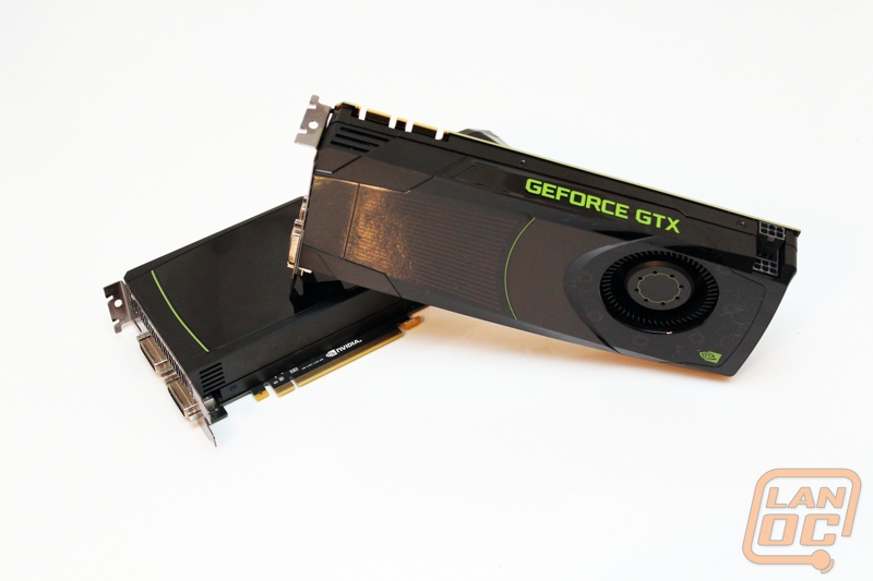
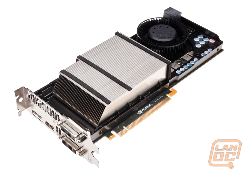
Here are full cards shots of the GTX 680, even in a reference design this is a good looking card. I love the use of the raised Geforce GTX logo up top with green highlighting it even more. I hope this carries over into other cards based on the reference design. It’s nice to be able to show off what you have inside through your side panel window.
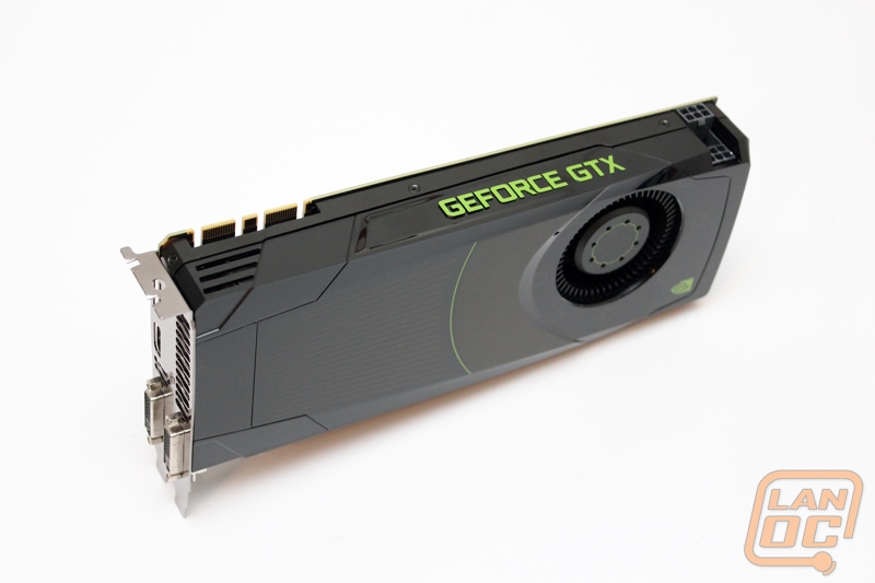
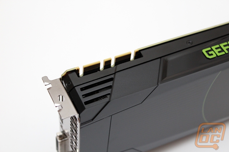
Being a flagship card this is no surprise really, but the GTX 680 is equipped with dual SLI connections. This means 3 and 4 way SLI are possible depending of the motherboard.
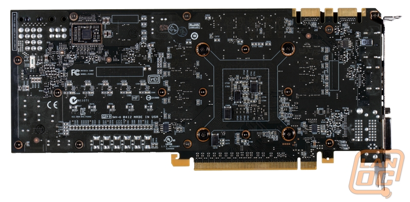
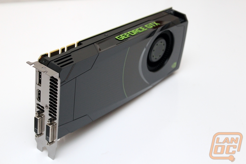
I have mentioned it before in this review already but here is a shot of the dual six pin power connections for the GTX 680. This is a very unique design but there is one problem that I ran into. The second connection is facing in meaning you have to have small fingers to poke down to the lower plug to hold the unlock tab on your 6 pin power connection to remove the cable. Nvidia mentioned that this layout allows them more room on the PCB for improvements and it also allows for the cards fan to be better placed.
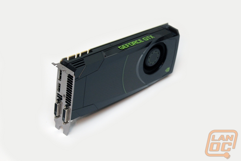
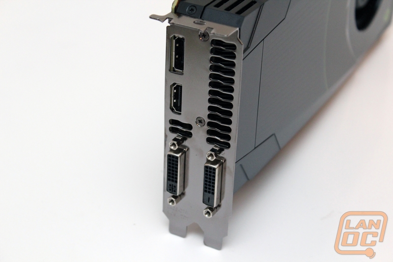
For connections here on the reference design we have two DVI, one HDMI, and a full sized display port connection. Nvidia packs as much ventilation as possible into the design also. They have pushed the vents almost up against the DVI port and they have also added a couple vents below the HDMI plug.
The side of the reference cooler has a nice indented section around the GPU fan; this will give the card room to breathe when it is packed up against other cards or with other devices. We have run into cards in the past without this breathing room and it can get a little too hot. It’s nice that NVidia has kept that in mind.
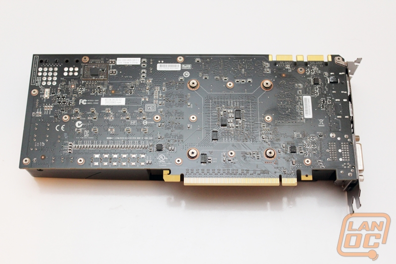
Here is the full back of the PCB. As you can see the card does not come with a backplate but they did got with a nice black PCB. The most noticeable thing that stands out to me on the PCB here is the collection of power connections up in the top left corner. Before NVidia said that they went with the stacked power connection design but you can actually see that they could have gone with ether connection (ignoring any cooling things to consider). They also have included enough connections for an 8 pin if needed. Are these left overs from a late design change or are we seeing power connections that could be used in future cards based on the same PCB? Only time will tell.
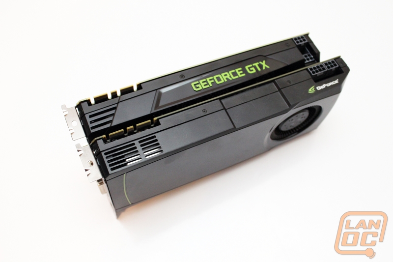
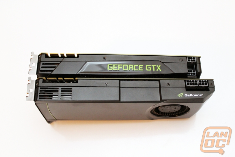
Here are a few shots of the GTX 680 paired up with the card it is replacing, the GTX 580. As you can see the new GTX 680 is actually a little bit shorter. Having that Geforce GTX embossed on the top of the card is a nice touch, especially when next to the GTX 580.
Our Test Rig
Asus Rampage IV X79 Motherboard
Seagate Constellation 2tb Hard drive
Cooler Master Gold Series 1200 Watt PSU
http://www.highspeedpc.com/ Test Bench
Kingston 1600Mhz DDR3 Quad Channel Ram
Kingston Hyper X 120 SSD’s in Raid 0
Our Testing Procedures
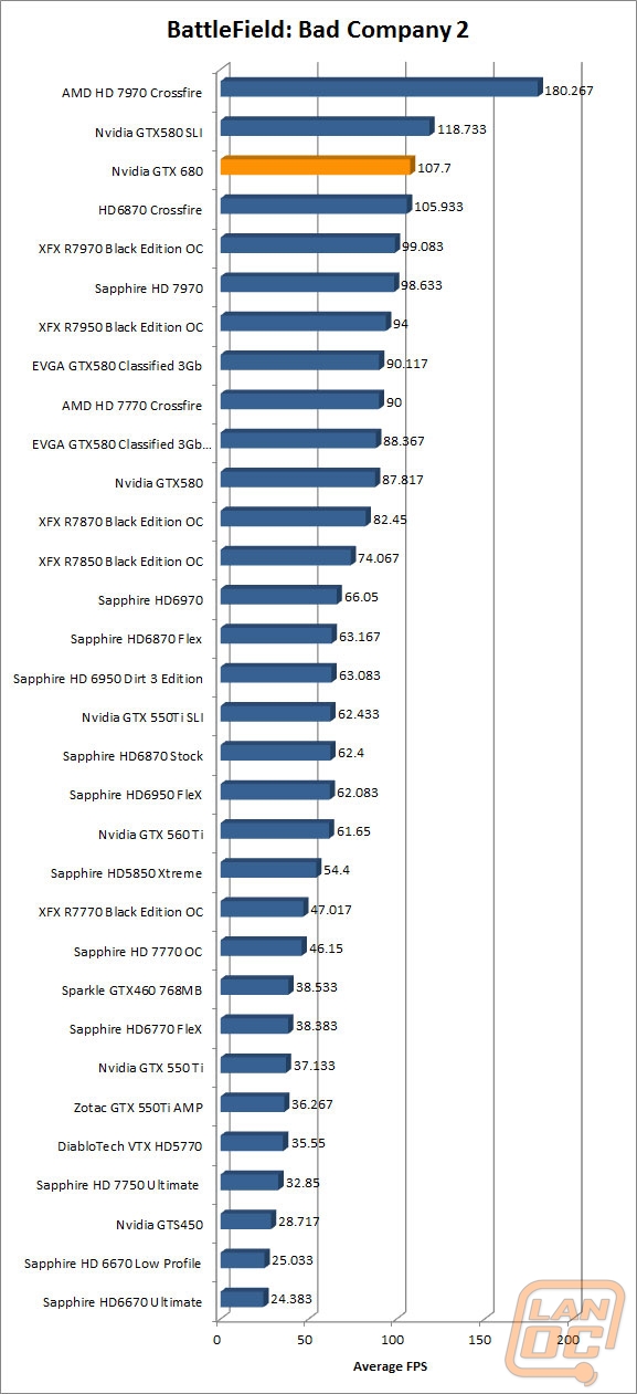
Battlefield Bad Company 2 (1920x1080 – high settings, first scene starting after the cut scene, recorded using fraps)
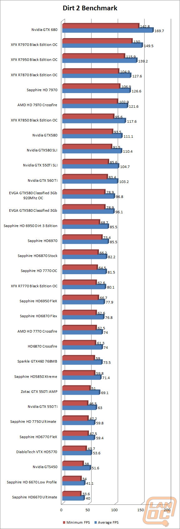
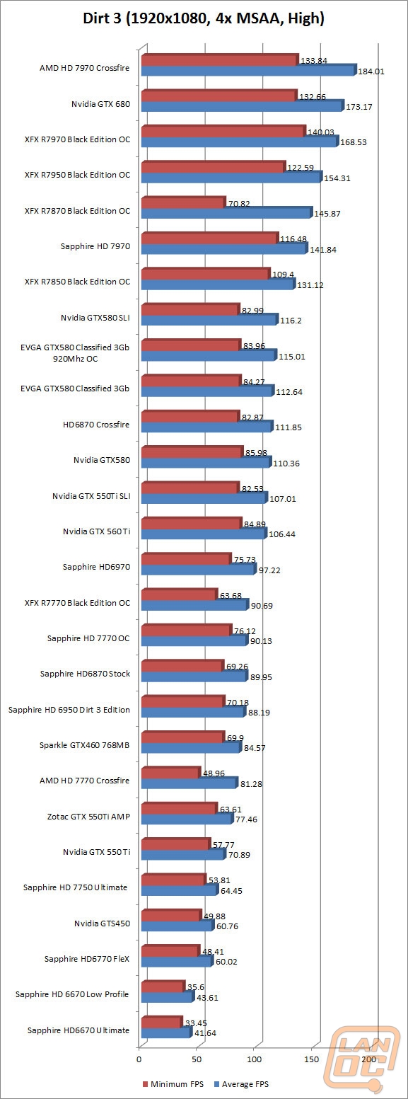
Dirt 2 (1920x1080 – 4x MSAA – high settings, in-game benchmark)
Dirt 3 (192x1080 - 4xMSAA - high settings, in-game benchmark)
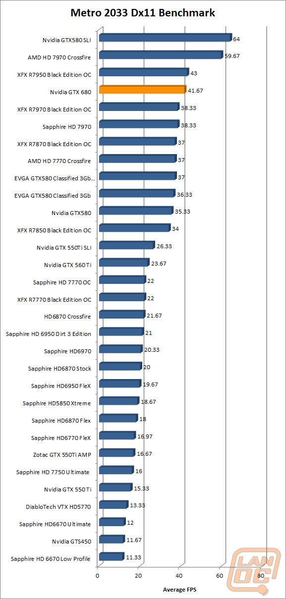
Metro 2033 DX11 (built-in benchmark, 1920 x 1080; DirectX: DirectX 11; Quality: Very High; Antialiasing: MSAA 4X; Texture filtering: AF 4X; Advanced PhysX: Enabled; Tessellation: Enabled; DOF: Disabled)
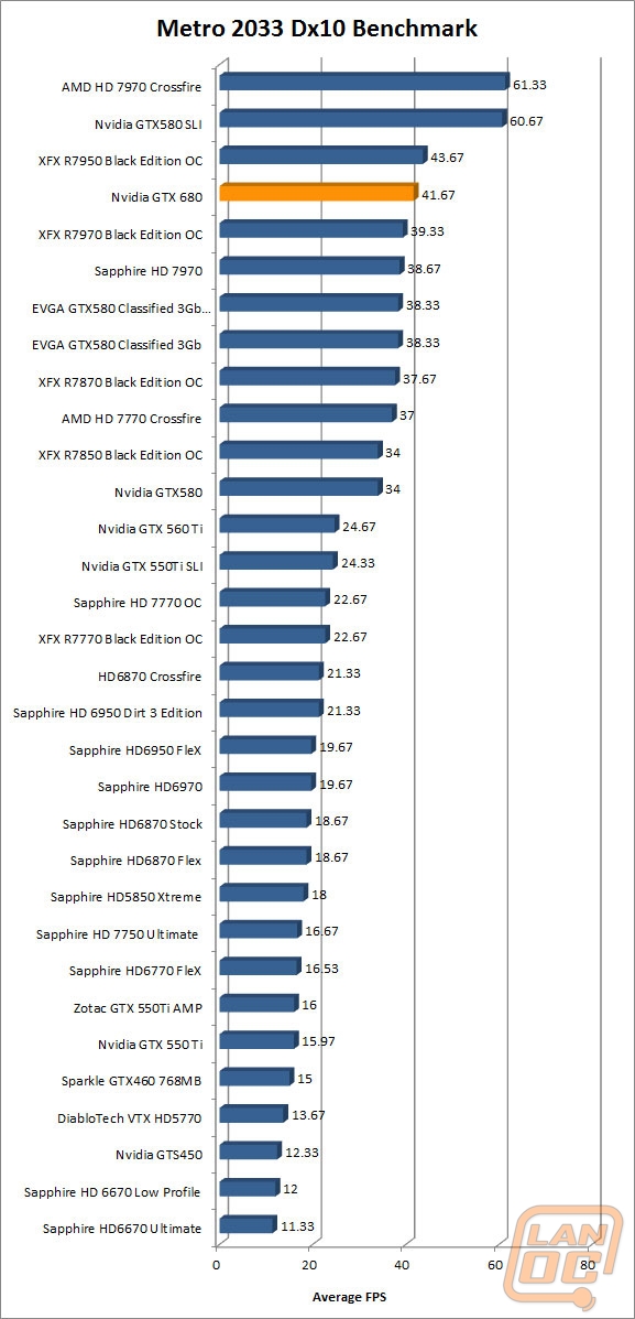
Metro 2033 DX10 (built-in benchmark, 1920 x 1080; DirectX: DirectX 10; Quality: Very High; Antialiasing: MSAA 4X; Texture filtering: AF 4X; Advanced PhysX: Enabled; Tessellation: Enabled; DOF: Disabled)
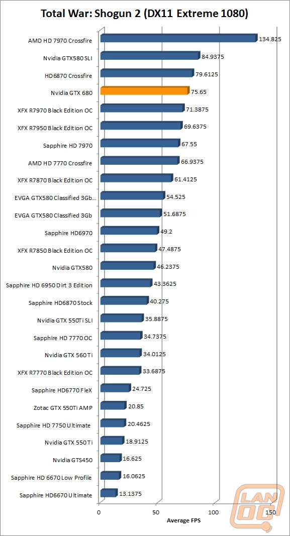
Total War: Shogun 2 Direct X11 Benchmark High setting
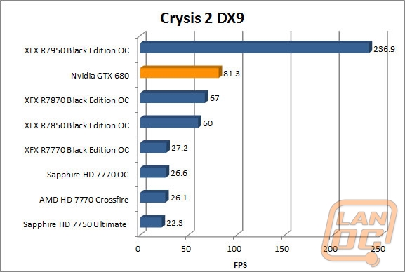
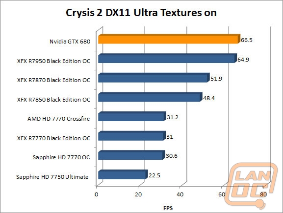
Crysis 2 Using Adrenaline Crysis 2 benchmark two runs. The first set of runs set to ultra-settings, 1080p, 4x Anti-Aliasing, DX11, Laplace Edge Detection Edge AA, on the Times Square map, with hi res textures turned on. The second benchmark set to Xtreme at 1080p, no AA, DX9, Edge Blur, Hi-Res Textures turned off on the Times Square Map.
Battlefield 3 Using Fraps with the game set to Ultra settings with 4x MSAA Antialiasing Deferred, 16X Anisotropic Filter, at 1920x1080.
Synthetic Benchmarks For video cards our synthetic benchmarks are limited to 3DMark Vantage and 3DMark Vantage 2011. 3DMark Vantage is run with PPU turned off with results from both the performance and high settings. In 3DMark Vantage 2011 we run both performance and extreme benchmarks
FurMark We use Furmark to push the video card to the limit and test its cooling performance. Keep in mind that FurMark pushes cards well beyond what they would ever do in game. Our tests are done using the built in 1080p benchmark.
Cooling and Noise
With Nvidia’s design for the GTX 680 being a very power efficient design I was a little excited to get the card into our Furmark 1080p benchmark to see how the new heatsink design works. Furmark pushes the card well beyond what you would ever be able to do in game. That means our results are going to be higher than you should ever see under stock clocks. But the idea is to make sure that you will never have your GTX 680 overheat at stock speeds and also to compare it to other cards we have tested.
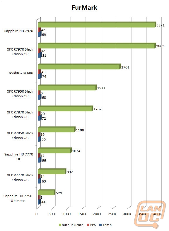
After running through the test we ended up with a max temperature of 74 degrees Celsius. For a stock cooler on a flagship card, this isn’t bad. We have seen higher temperatures from the AMD side of things, even with aftermarket coolers.
While doing this testing we are able to get a good listen to both the cards idle noise levels and how loud to expect it to be when it’s at max load. At both idle and max load I was impressed with the GTX 680’s noise level. At idle the card was nearly silent; considering our open air bench gives us an up close listen to the card this is very impressive! It’s even more impressive when you add in that this is a reference design; it really is amazing how far they have come in the last few years. When loaded up there is obviously more noise output but it’s better than one would expect and actually less than what we have seen on any other reference coolers to date.
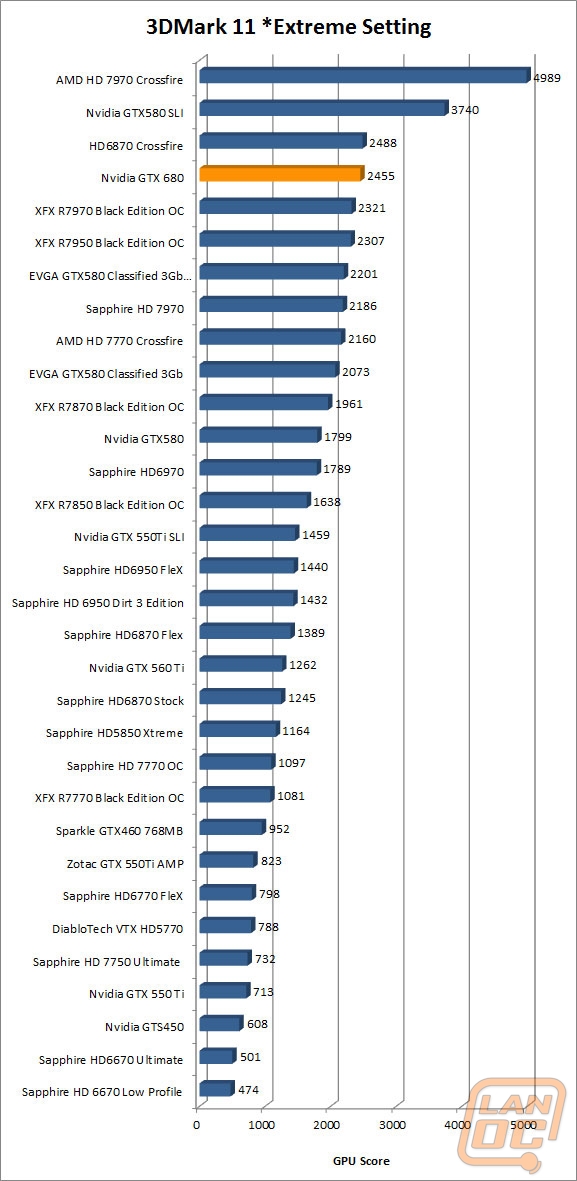
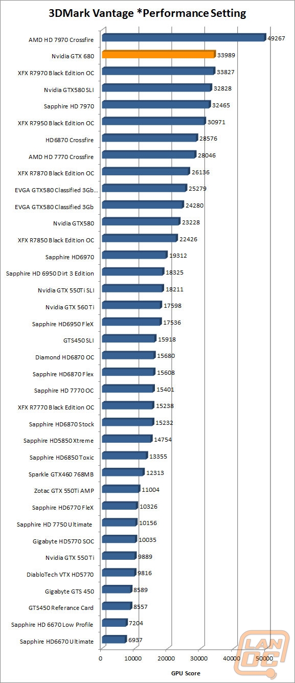
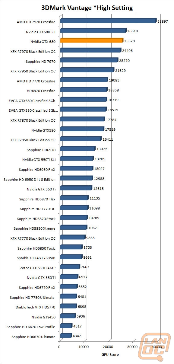
3DMark
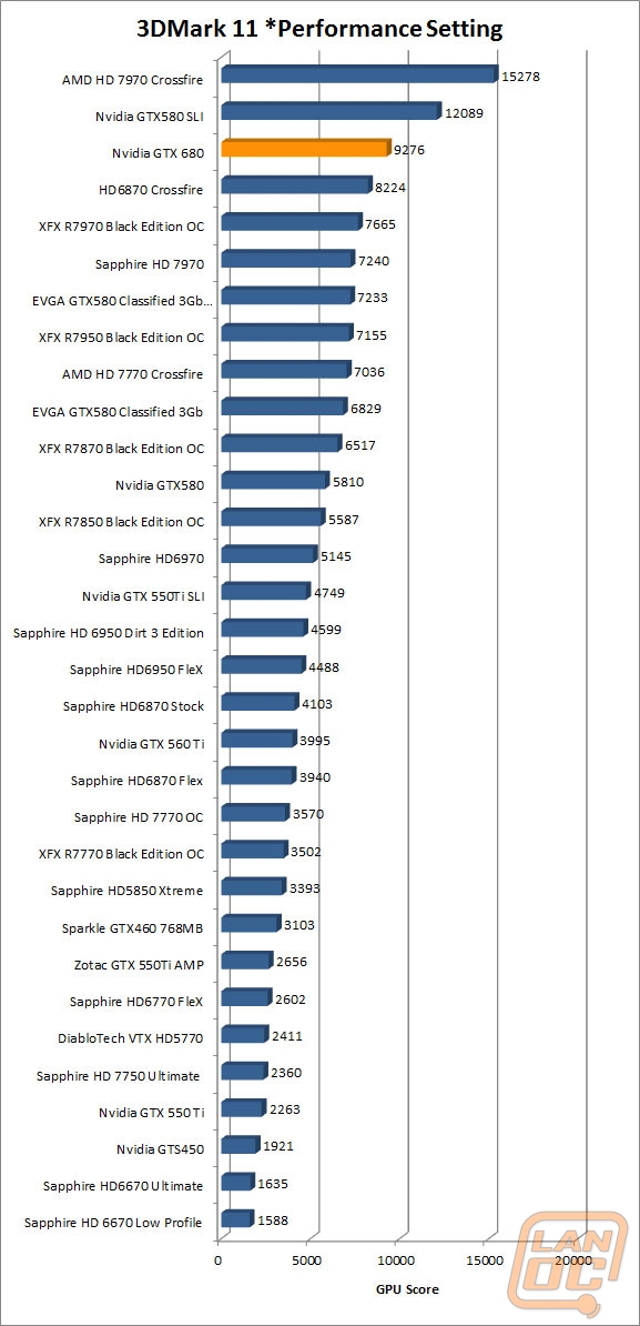
Our 3DMark benchmarks may not tell you how well a card is going to perform on any specific card, but because they are so consistent we can compare between cards easily. In this case, and in all four of our 3DMark tests, the GTX 680 just smokes every single card we have tested. The only competition for the GTX 680 are a few SLI and Crossfire solutions, and even then it’s only when you pair up multiple high end cards.
Just to give you guys an idea of where the GTX 680 stands. On 3DMark 11 Performance it out performed the overclocked R7970 by a full 21% and the 1.5 gig GTX 580 by almost 60%! In our testing on the older 3DMark Vantage the gaps were much closer, with the GTX 680 just barely beating the overclocked R7970.
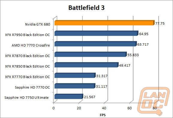
In Game Performance
In game performance numbers for the GTX 680 are an exercise in overkill. In some cases like Dirt 2 and 3 was saw numbers up beyond 130FPS, more than enough for perfect 3D gaming running at over 60 FPS. Considering the big gaps in performance between the GTX 680 and AMD’s options in 3DMark I was a little disappointed to see it only beating the R7950 by around 17%, not that that isn’t a nice increase. Frankly 77+ FPS in Battlefield 3 at the settings we are testing is very impressive, I can’t wait to see what two GTX 690’s will do in SLI.
Overclocking
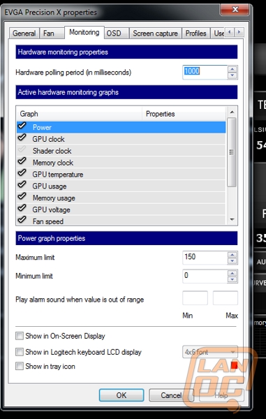
As I mentioned before overclocking the GTX 680 is a whole new ball game. Nvidia’s new GPU boost itself means when you’re overclocking your trying to hit a moving target. That is because even before overclocking it really depends how you are putting a load on the card as to how high your clock speed will be. Then on top of that you have a couple different ways to work on your overclock now in EVGA’s precision that are nothing like what we have seen in the past. Let’s quickly go over them so you can understand what we are working with.
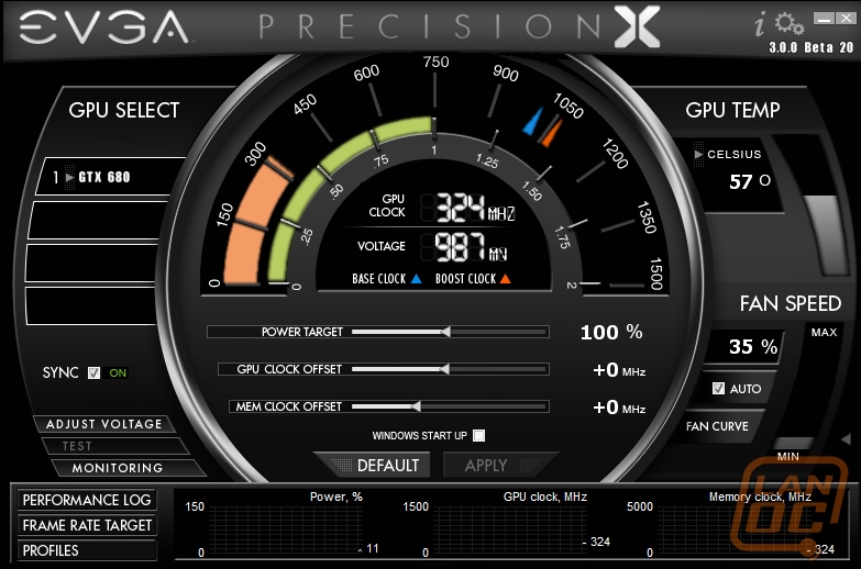
You have seven different variables you can adjust, precision X has laid them all out in an easy to use way. The first three and the most important are right in the middle (Power Target, GPU Clock Offset, and Mem Clock Offset). Then to the right you have fan speed and also fan curve. On the left side there is a button for adjust voltage that brings up EV Tune. Last you have Frame Rate Target.
Thre first three are what you will use the most. Setting Power Target will adjust the amount of power the card will push to use when using GPU boost. The stock TDP is 195 Watts, adjusting up or down is similar to playing with the turbo on an Intel CPU but without the ability to set a specific MHz. GPU Clock Offest and Mem Clock Offset are very similar so we will group them together. This is where you can turn up your base clock speeds. This may be a little confusing to some because this isn’t actually setting your total overclock. You have to combine both your power target and your GPU/Mem offsets to get your overclock. This is because no matter how far you turn up your overclock the card won’t let you use more than the power target, in this case 195 watts.
The fan adjustments are fairly simple. You can crank the fan speed up to whatever you would like or turn on auto. With auto set you have the ability to jump in and adjust your fan curve meaning you can make the card quiet until it needs the cooling.
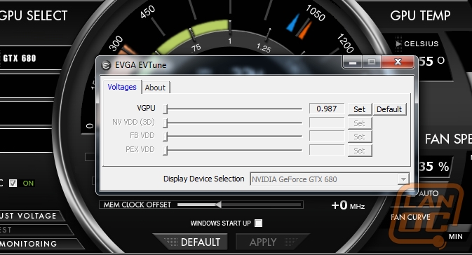
Adjust Voltage is exactly as the name describes. You can adjust the VGPU voltage up or down in a short range. It’s nice to see this packaged in with precision making overclocking even that much easier.
The last option is Frame Rate Target, this one may be a little confusing to some. Basically you are setting you’re in game FPS goal and the card will overclock (slightly) to reach this goal. When your performance is more than enough it will actually turn the card down to keep heat, noise, and power usage down. This may seem like crazy talk to some who would want the performance ALL of the time. But this is a very efficient way to do things. The overclock is adjusted every 100ms depending on what you need and what the card can handle at that moment.
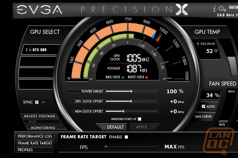
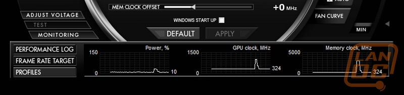
So now that you know what we are working with how did the GTX 680 do? Once you get past all of the new ways to overclock it was actually very easy. I was able to see a clock speed of 1346 Mhz when running 3dmark 11 performance but when going back and looking at the logs the card was pulling back on the clocks, even with the fan turned up to its max setting of 80%. Adjusting our settings down slighting to 1316 yielded a consistent speed without the card having to intervene. This is of course all with the stock reference heatsink. I’m really excited to see what everyone will be able to with more exotic cooling solutions!
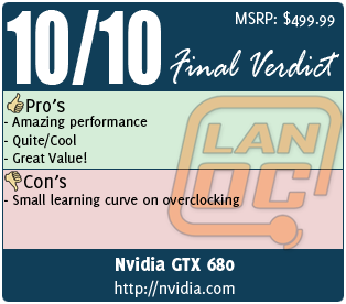
Overall and FV
When NVidia invited me out to check out what they had been working on I was excited but unsure of what to expect. They had been very quiet about what to expect up until that point. After getting the full breakdown their and heading home to put the card to the test I have been very impressed with both the performance of the GTX 680 but also the work that NVidia put into both the card and the software and drivers behind it. Performance is one thing, but the dynamic boost that GPU Boost give you is unique and efficient in design and implementation. Adaptive VSync and the improvements in surround show that NVidia is always trying to improve our gaming experience by listening to what everyone wants and what everyone hates about PC gaming. Being able to run 3+1 on one card is a big step in the right direction.
So I’m sure by now you’re wondering what it’s going to cost you to get a GTX 680 into your new PC right? What would you pay to get the fastest single GPU on the market? For the last few months the HD 7970 reference card has been selling for $549 and the GTX 680 out performs it considerably. I was very surprised when NVidia let us know that the GTX 680 will retail for $499. That is a price that even as lesser performance would/will force a major change in pricing for all video cards on the market. This is exciting because this will mean better performance for your dollar across the board. I expect to see a lot of people sporting GTX 680’s in SLI at that price, especially as they mature a little bit and we see even lower prices.


")